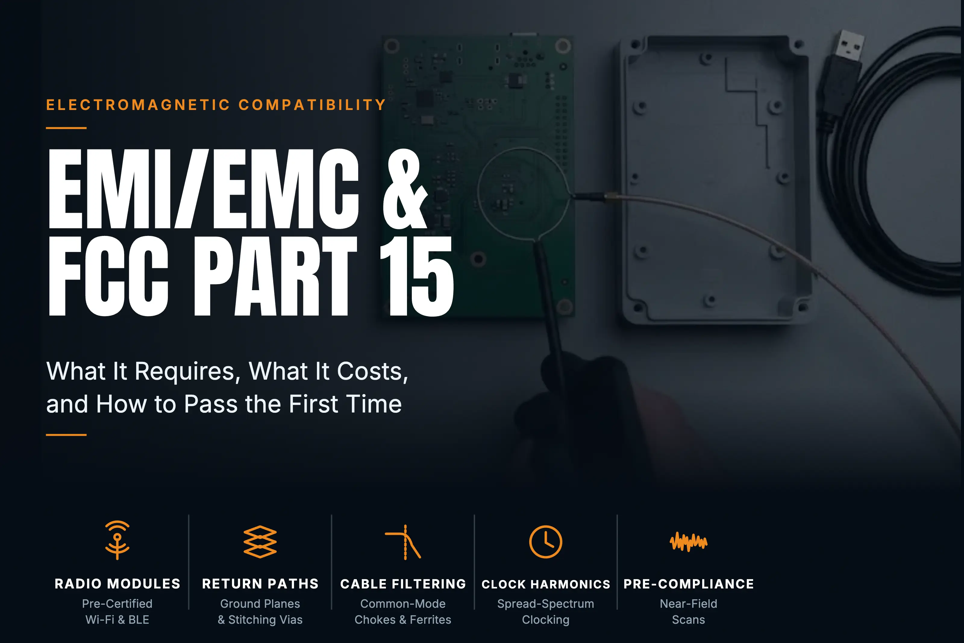
FCC Part 15 compliance is the legal requirement that nearly every electronic product sold in the United States must not pollute the radio spectrum. For product design teams, it's the kind of exam you can't skip, reschedule around investors (at least not without seriously pushing back product release dates), or argue with. The engineering discipline whose application is what causes your device to pass or fail it is called EMC (electromagnetic compatibility) design, and the key to winning the game is when you start: EMC designed in from the beginning costs comparatively much less; EMC retrofitted after a design has otherwise been declared “complete” costs significantly more time and money.
This guide explains what Part 15 actually requires, what testing costs, why boards fail, and the design tactics that minimize your time in a compliance lab.
FCC Part 15 compliance - key takeaways
- FCC Part 15 compliance applies to the majority of consumer electronic products and medical products (as well as a high percentage of industrial and laboratory products) sold in the US. Saying, "We're not a radio product" only narrows which rules apply, not whether at least some of them do.
- Designers creating products that are unintentional radiators (this covers most digital products and some analog ones as long as there is no transmitter in them) can self-declare after verification testing at an accredited lab. Intentional radiators (anything with Wi-Fi, BLE, cellular) need more extensive certification. Using pre-certified radio modules may shrink that burden, although it may not allow you to avoid intentional radiator testing altogether. Remember that the FCC isn’t grading you on your component selection, they’re grading you on whether your entire device meets the applicable regulatory requirements.
- Formal testing for simple emissions from an unintentional radiator typically runs in the thousands of dollars. For devices with radios, testing costs more (usually starting in the low tens of thousands). The higher cost structure for testing particularly applies to those radio devices that aren’t part of a module that has itself been qualified somehow. More often than not, a failed test adds a board respin and typically takes another 3-5 months of calendar time. A high percentage of failures are layout failures. Broken return paths, cables acting as antennas, and unfiltered I/O account for the large majority of over-limit results.
- Pre-compliance scanning - from a comparatively inexpensive near-field probe setup to a day at a pre-scan lab - finds problems while they still cost hours, not calendar quarters. As is the case with UL certification for safety, if you can possibly engage the people who will be doing your EMC testing while the design is still open to change, it’s highly recommended that you do so. Many of them have been in the compliance testing business for decades, and they’ve seen it all. Leverage their expertise whenever possible.
- EMC is a system property: The board, enclosure, cables, firmware, and clock distribution all participate, so saying "the PCB passed" means little unless the entire product passes.
- Design review before fabrication beats trying to patch things over while debugging in the lab. It pays to put the EMC review where the schedule can still absorb its findings. And if you’re reading this now, congratulations, you’re already thinking about something that many people completely ignore in their enthusiasm to get to a prototype. To quote one of our own favorite office comedians, “We don’t want to have a duh-lay.”
What FCC Part 15 actually requires
Part 15 of the FCC rules divides the world in two:
- Unintentional radiators - products (usually with digital circuitry) that don't transmit on purpose: instruments, controllers, appliances, anything with a clock much over a few kilohertz. These must stay under conducted and radiated emission limits, demonstrated by testing, and self-declared under the Supplier's Declaration of Conformity (SDoC).
- Intentional radiators - anything with a transmitter: Wi-Fi, Bluetooth, cellular, proprietary RF. These require certification through an FCC-recognized Telecommunication Certification Body, with test reports, filings, and an FCC ID on the label.
Two classifications matter within the limits: Class A (commercial/industrial environments) and Class B (residential - roughly 10 dB stricter). Selling into homes or offices means Class B. It’s best to design to Class B requirements unless you're certain of your sales channel forever. Willy Wonka may be making chocolate in a factory, but the minute he takes home your instrument to bake brownies in his own kitchen, you may have a problem.
IMPORTANT: Using a pre-certified radio module (a certified BLE or Wi-Fi module with its own FCC ID) usually lets you inherit the module's radio certification and test your product as an unintentional radiator - often saving months and thousands of dollars in development and test. The catch: you must follow the module vendor's antenna and layout integration rules exactly, or the inheritance is void. This is the single highest-leverage certification decision in most connected products, and it's made at architecture time, not in the lab.
Exports add siblings: the EU's CE/RED regime, Canada's ISED, and others - the good news is that a design that passes Class B with margin usually travels well.
Why boards fail EMC
An EMC failure is physics finding the antenna you built by accident. The usual suspects, in rough order of frequency:
- Broken return paths. Every fast signal's return current wants to flow directly beneath it. Route over a plane split or change layers without a stitching via, and the detour loop radiates. This one failure mode explains more over-limit scans than any other - and it's free to avoid at layout time. (It's the same physics that makes high-speed interfaces fail, which is why EMC and signal integrity are one discipline wearing two hats.)
- Cables as antennas. The board is small; the USB cable is a meter of wire fed by whatever common-mode noise your I/O carries. Unfiltered, unshielded, or badly grounded cables turn a quiet board into a loud product.
- Clock harmonics. That spike at 480 MHz is rarely mysterious - it's the 20th harmonic of a 24 MHz clock, radiated by a trace, a heatsink, or a slot in the ground plane that happens to resonate there.
- Power delivery ringing. Switching regulators with loops laid out in excessively large PCB patterns or digital rails without local decoupling spray broadband noise into everything - and often out through the cables.
- Enclosure surprises. Seams, display cutouts, and ungrounded metal panels turn "shielded" enclosures into slot antennas at exactly the frequencies at which the slots resonate. A 480 MHz pulse from a USB data line has a quarter wavelength of about four inches – just the size of a lot of panel cutouts.
Designing to pass: the tactics that matter
At architecture time
- Choose pre-certified radio modules unless RF is your core competence and volume justifies custom certification.
- Think through the enclosure strategy (plastic vs. metal, sizes and shapes of cutouts, etc.). It drives both cost and layout tactics.
- Spread-spectrum clocking on processors and any switchmode devices, where the silicon offers it, buys 2–6 dB of peak reduction for free, if it's selected early. Do a thorough reading of the datasheet for a buck or boost converter, since many will run in more than one mode, and you may want to trade conversion efficiency for relative RF quiet. Even the least efficient of switchers these days can manage over 90% efficiency at anything other than the lightest of loads (where efficiency matters least, anyway).
At layout time
- Unbroken ground planes adjacent to every fast routing layer; stitching vias at every layer transition; no routing over splits. Non-negotiable.
- Contain the larger current loops: Create switching regulator layouts per the vendor app note, minimizing loop areas. Place input caps first, not "where they fit" after the fact.
- Filter every cable interface: Use common-mode chokes, ferrites, or π-filters at connectors, with component pads designed in even if you hope to DNP them. An unpopulated filter footprint costs nothing; a missing one costs a respin.
- Keep clocks and radios apart from I/O regions, and give crystals and RF feeds the ground-pour discipline the datasheets ask for.
Before the formal laboratory examination
Pre-compliance testing is the cheapest insurance in electronics. Levels of investment:
- Bench probes (Typically $1K to $3K, depending on where it’s done): Near-field probes plus a spectrum analyzer (even a modest one) will find your worst emitters and rank your fixes.
- Pre-scan day at a lab (Typically $3K/day): Done informally but in a real chamber. Your engineer should be allowed to touch the product mid-scan. One day here typically resolves more than a month of speculation.
- Formal testing (Usually in the $10K-$30K range, depending on the lab and the complexity of your design) always to cover unintended emissions and costing more with radios and immunity suites: This is the graded exam. Arrive having already passed the practice tests.
WARNING: Test the product, not the board - final enclosure, real cables, real accessories, worst-case operating mode (all radios on, display active, motors running). A bare board that passes tells you very little about the boxed product that ships.
The pre-compliance checklist
Before booking the formal scan, confirm:
- You have all cable interfaces (filtered or shielded), tested with the cables that ship in the box.
- You have reviewed ground stitching at every high-speed layer change.
- You have audited any switchmode power converter layouts against vendor application notes.
- You have grounded enclosure seams and cutouts per design, not per hope.
- You have any firmware pinned to the worst-case emissions mode for testing (and that mode is documented for the lab).
- You have completed a near-field scan or done a pre-scan day, your worst emitters are known, and their effects have been mitigated.
- Labels, user manual statements, and (for SDoC) the US responsible-party designation have been fully and properly prepared. Paperwork failures delay approvals as effectively as emissions do.
How Focus Embedded can help
We design boards to pass the first time - because our layout practice treats EMC and signal integrity as one discipline, applied before fabrication rather than after the lab report.
We do EMC-aware hardware design with:
- Digital and analog design with filtering and grounding strategy designed in
- Advanced PCB layout with return-path discipline and controlled emissions as explicit design constraints
- High-speed interfaces (DDR, PCIe, USB, MIPI) engineered for FCC Part 15 compliance from the stackup up
- Design reviews of existing boards headed to (or back from) the lab
Why work with us:
- ✅ Hardware shipped into unforgiving environments - from light-aircraft instrumentation to a smart oil-pipeline flow valve - where emissions and immunity are reliability issues, not just paperwork
- ✅ Layout and circuit design in one team: EMC fixes go into the schematic and the stackup, not just into a smattering of ferrite beads sprinkled at the end
- ✅ Honest triage: if your failing board needs a $200 filter change and not a $40k redesign, that's what we'll tell you
Ready to pass on the first visit?
Talk to an engineer, not a salesperson. Whether you're designing for compliance or holding a failing lab report, tell us where you are and we'll tell you the shortest path through.
📞 +1 (512) 246-9012 (or 1-888-FOC-7924) 📧 info@focusembedded.com 🌐 focusembedded.com/contact
Summary
- Part 15 applies to essentially everything electronic sold in the US; radios change the paperwork, not the obligation.
- Most failures are layout failures - return paths, cables, clock harmonics - and all of them are cheap to prevent and expensive to retrofit.
- Pre-certified radio modules are the highest-leverage certification shortcut, if you follow the integration rules exactly.
- Pre-compliance scanning converts EMC from a launch-week lottery into an engineering task with a known answer.
- Test the boxed product in its worst-case mode - that's the thing you're actually shipping.
The lab doesn't grade on effort. Design so the physics is on your side before you book the chamber.
Related articles
- High-Speed PCB Layout: DDR, PCIe, USB & MIPI Without the Respin
- Embedded Software Development Services: What They Are (And How Not to Pick the Wrong Partner)
