
The prototype worked on the bench. Then the second batch arrived from a different fab lot, and a third of the boards began throwing memory errors as they warmed up. The schematic didn't change. The BOM didn't change. What changed is invisible: a few mils of dielectric, a slightly different glass weave - margins that a marginal layout had already spent.
High-speed PCB layout is the discipline of designing boards where the copper itself is a circuit element - where trace geometry, stackup, and via placement determine whether DDR memory, PCIe, USB 3, HDMI, MIPI, or other high-speed interfaces run with comfortable margins or run on luck. The line between "digital" and "high-speed" isn't strictly clock frequency. It can be a whole lot of other parameters (notably edge rate) that make themselves known in the frequency domain in places you'd least expect. A square wave, after all, has a sinc function for its Fourier transform. A 48 MHz microcontroller with 1 ns risetimes is a high-speed design whether you treat it as one or not.
This guide is for the person who pays for the respin: what actually makes a layout high-speed, the rules that matter per interface, and the red flags that tell you a layout quote doesn't include the engineering your interfaces require.
High-speed PCB layout - key takeaways
- High-speed PCB layout treats traces as transmission lines - controlled impedance, matched lengths, managed return paths - and it starts at the stackup (or even before then with a conversation with a PCB fabricator about his process), not at routing. A competent design team will work with a board maker to determine the trace and space widths on each layer and match them to the dielectric material and the thicknesses of the board "pre-pregs."
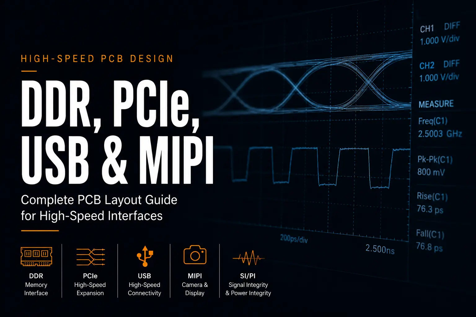
- Often, parameters such as edge rate (far more than clock frequency) define what constitutes "high-speed". In many cases, signals with short rise times will require impedance control regardless of their overall frequency. One has to consider what is happening in the frequency domain – and that other than pure sinusoids, all signals are built up from at least two sine/cosine variants of different frequency and amplitude from the fundamental frequency. Digital signals, usually being square at their edges (or at least sufficiently non-sinusoidal when viewed on an oscilloscope), may well present something like an "eye pattern," where if data are to get through unmolested, the eyes have to be open. What keeps them open is the presence of higher harmonics that give sharpness to the signal edges.
- DDR variants are among the least forgiving common interfaces, requiring line length matching not only for signal pairs but also within an overall data/address port comprised of multiple paired signals. Interestingly, later (and faster) variants of DDR are slightly more tolerant of line length mismatches due to their ability to support better "training algorithms" that de-skew signals with circuitry inside the chips that can alter signal phasing. (When NASA needed a company to route older variants of DDR for an interplanetary rover, they called Focus Embedded. In the harsh conditions of space, older (and larger geometry) transistors are needed to withstand the bombardment of solar winds, as a 90nm transistor can take a much harder whack from a charged particle than a 15nm transistor can. We've been doing this work since the bad old days when the chips themselves offered little to no help deskewing signals.)
- A failed board spin can cost as much as tens of thousands of dollars in direct cost and usually at least four weeks (and sometimes ten or more weeks) of calendar time. More importantly, if time to market is an issue, one respin usually exceeds the price of having the layout done right in the first place.
- Return paths often get far less attention than they should. Most designers know not to route signals over split planes – at least not without some mitigation of the effect of the crossing (with stitching to other ground planes, for example), if there's absolutely no other choice. But it's always worth remembering that current always flows in a loop. Better it should be a loop with a path you planned than one you didn't.
- A proper set of design rules built into the layout tool before place and route begins can save a staggering amount of misery later. And it will usually accelerate the "design rules checking" that any competent board shop will do when it gets a set of Gerber files for making the board.
- Your layout is only as good as its fab notes: impedance control must be specified, tolerated, and coupon-tested, or the fab is free to give you nominal geometry instead of nominal impedance.
🕒 Board already misbehaving? Talk to an engineer, not a salesperson → contact Focus Embedded
What makes a layout "high-speed"?
At low speeds, a PCB trace is a wire: it usually connects one or more components, and its shape is irrelevant. Close to DC, as long as one need not be concerned with the ampacity of traces and/or PCB heating (and additional current constraints that may drive higher copper weights in the board's fabrication), it's reasonable to treat the PCB's copper routes as ideal conductors that are in no way circuit elements themselves. For lower-current signals, above a threshold - often set by edge rate and trace length - the trace becomes a transmission line, and three new physical realities take over:
- Impedance: the signal sees the trace's geometry (width, dielectric height, copper thickness) as an impedance. Mismatches reflect energy back, doing everything from corrupting signals to unlocking phase-locked loops. Interfaces specify their impedances (for example, 50 Ω single-ended, 90–100 Ω differential, etc), and to meet those, a stackup of PCB layers and space/trace widths are chosen to arrive at the correct square root of inductance over capacitance.
- Return currents: every signal current returns to its source, and at high frequencies it often returns directly underneath the trace, in the reference plane. Split that plane, or change layers without a nearby stitching via, and the return current detours - creating emissions (an EMC problem), crosstalk, and edge degradation, all at once.
- Timing skew: A signal covers roughly 6 inches per nanosecond in FR-4. Length mismatches inside a bus become timing errors. So do vias: one via adds delay comparable to ~15–70 mils of trace, which is why one must set one's design constraints carefully inside the PCB layout software..
IMPORTANT: These effects cause failures that are frequently intermittent and non-repeatable, which are the most difficult kinds of bugs to chase. A marginal high-speed layout can works on the bench - at room temperature, on the first fab lot, with this week's DRAM stuffing option. Later, it fails statistically at volume: in the field, at temperature, on the lot with slightly different dielectric. Over the years as silicon component geometries shrink at the wafer fabs, the chips themselves, with identical part numbers to those that worked before in a circuit, start misbehaving. That's what makes marginal layouts so expensive - they pass prototype debug and fail in production. Often, they do so after years of manufacture, when the engineers who originally designed a system have long since forgotten what they were doing – or have moved on to other employment, retired, or perhaps even died.
The stackup
The stackup isn't the whole design, but it's certainly a piece of the structure that if rotten will guarantee that some day the entire house will come crashing down.
Amateur layouts start with routing. Professional high-speed layouts start with a stackup negotiation between the design and the fab, because every impedance target is a function of layer geometry the fab has to actually build.
A serious stackup process looks like:
- Count the routing layers the interfaces need. A DDR4 fly-by bus plus PCIe lanes isn't the stuff of four-layer PCB's, even if a simple USB2.0 connection (which still has it's own 90 ohm impedance and time-of-flight constraints) might be. Six layers might work, but it would be a major test of a designer's skills. With eight layers, there's a lot more breathing room.
- Assign reference planes so every high-speed layer has an adjacent, unbroken ground if at all possible. If it's not possible, be prepared to add stitching vias and consider your outbound and return routing paths exceedingly carefully.
- Get the fab's real dielectric menu and compute trace geometries for each impedance target. Serious, competent
- Put impedance control in the fab notes - target, tolerance (±10% standard, ±7% or better for demanding interfaces), and a test coupon requirement, so the fab certifies impedance, not just geometry. IPC-2141 and the IPC-2220 family cover the controlled-impedance design ground rules the industry works from.
Per-interface rules
What actually matters is where high-speed layout reputations are made and lost, and it's why we treat each type of circuit largely as its own specialty within our advanced PCB layout practice, even if they do have a great deal of commonality.
For DDR:
- Topology: DDR3/DDR4 address/command runs fly-by to each DRAM (with ODT doing the termination work); data byte lanes route point-to-point. LPDDR4's lower voltage swing buys power savings but pays for it in tighter margins.
- Length matching within byte lanes: DQ to DQS matching within a lane is typically held to ±5–25 mils depending on speed grade - and it must be delay matching that accounts for vias, not just trace-length arithmetic.
- Training algorithms only buy you so much: On-chip timing controllers can calibrate away some skew, but calibration range is a budget, and a sloppy layout can spend all of it before temperature and voltage margins also take their share.
- Follow the controller vendor's layout guide closely. If nothing else, most of the major memory makers publish DDR routing rules for their parts down to via counts per net. Deviate from these, and you will be in the inescapable realm of "it mostly works." Often chipmakers will present sample layouts in their data sheets, and those are well worth taking to heart. Silicon foundries take this work very seriously, since they know their silicon (in their packages, which have complex impedances of their own at speed) will get used in staggering numbers of different designs. Focus Embedded regularly works with one especially well-known east Asian supplier of foundry services for dozens of "fabless semiconductor" companies (and companies which do have fabs but which don't want to run certain processes in-house). So we can attest to just how seriously the guys designing the chips (and choosing their packaging technologies) are when it comes to getting reliable specifications out to their customers. When they need a PCB to verify that the model for their giant uBGA accurately reflects reality, we get called to provide in, and in the process we get a window into their world.
PCIe - Offers some level of forgiveness, but it's only within limits
PCIe's embedded clocking and equalization made it, in some respects, marginally more tolerant of borderline layout than DDR. This was, of course, until PCIe reached Gen3/Gen4 rates, where timing budgets shrink quickly.
- 85–100 Ω differential (per spec revision), pair-matched to a few mils; The intra-pair matching matters. The concern between pairs is more one of crosstalk.
- AC coupling caps sized and placed per spec, with the pad voids the geometry needs at higher rates.
- Minimize via stubs with better routing and (if necessary) backdrilling: At Gen3+ speeds a long via stub is a resonator sitting exactly where your channel needs overshoot and ringing the least. It's also an antenna and can get in the way of FCC Part 15 compliance.
- Make use of the freedoms to polarity-invert and to reverse lanes if need be. Ideally, with good parts placement and enough open routing lanes, exploiting them can be kept to a minimum. But they do exist to save your routing; use them instead of attempting to make a complex or awkward signal crossovers if you have a choice.
USB 2.0 / USB 3.x - can be deceptively routine, particularly if running no faster than full-speed.
(Most designers do tend to pay more attention when clocks get over 12MHz.)
USB 2.0 (90 Ω differential) tolerates a lot, which is exactly why it's the most commonly botched interface: it gets no respect. USB 3.x SuperSpeed pairs at 5–10 Gbps deserve full SERDES discipline - loss budgets, stub control, and clean references - plus real ESD protection placed at the connector, picked for low capacitance so the protection doesn't destroy the eye it protects.
MIPI DSI / CSI-2 - short, dense, unforgiving of noise
Display and camera links (typically 100 Ω differential, D-PHY) usually run short distances but through the most congested regions of the board, next to switching power and RF.
- Keep lanes tightly matched to their clock lane and shielded with grounds from noisy neighbors.
- Flex-to-board transitions (nearly universal for cameras and displays) are impedance discontinuities by construction - design them, don't inherit them. And begin a conversation with the maker of your flex circuit early in the design process. The number of PCB manufacturers specializing in flex circuits is quite a bit lower than the number doing rigid boards, and those that have undertaken the manufacturing of flex PCB's have put a lot of work into honing their processes. They're a great resource and can be of considerable help if you let them in on the design phase and don't simply throw a stack of Gerber files over the wall at them.
Common high-speed layout mistakes (the respin catalog)
1. Routing over plane splits
Mistake: a high-speed trace crosses a gap in its reference plane. Consequence: the return current detours, radiating (hello, failed FCC Part 15 test) and degrading the edge. Fix: unbroken reference under every high-speed net.
2. Length matching without via awareness
Mistake: CAD says the bus is matched to ±5 mils; half the nets have two vias, half have none. Consequence: real skew several times the "matched" figure; margins silently spent. Fix: make the most of design rules built into the CAD software so a mistake is caught at the moment it's made, match by delay, count vias, and verify with post-layout simulation.
3. The unnegotiated stackup
Mistake: impedance calculated on a textbook stackup before the fab starts making substitutions to make the board manufacturable. Consequence: The design works with one fab and fails with the second source. Or someone orders a different set of pre-pregs and suddenly marginal signals become a problem. Fix: design on the fab's real materials; require coupon-verified impedance in the notes, even in production, not just in prototyping.
4. Decoupling as decoration
Mistake: capacitors placed where there was room, connected by long thin traces. Consequence: power rails sag on transients; the DDR bank that "randomly" fails is often responding to your power integrity, not your signal routing. Fix: placement and via connection per the power-delivery analysis, not per aesthetics. Sometimes this will mean using a smaller passive part package to get something to fit properly. Check with the final PCBA assembler as to what works for him. Nearly everyone today can handle 0402-sized passive components. Not everyone can deal with the 0201 package, and some folks who can don't particularly want to. By the time you're below 0201, you're likely into some of the higher-end assembly shops, so consider where you're going to get things built.
5. Connector and ESD afterthoughts
Mistake: protection devices added late, wherever they fit. Consequence: either no protection in the current path, or so much capacitance the interface "eyes" begin to close. Fix: Make protection a part of the channel design from day one.
How do you buy a high-speed PCB layout - and what can be reasonably expected to be included?
When comparing layout quotes, make vendors state which of these will be part of the package:
- Stackup design with the target fab, including impedance and material selection
- Constraint setup (impedances, matched groups, spacing rules) in the CAD tool, reviewable as a file, not a promise
- Post-layout signal-integrity simulation for DDR and SerDes channels
- Power-integrity analysis for the core rails
- DFM review with the fab and assembler before release
- Fab notes with impedance tolerances and coupon requirements
A quote that's 40% cheaper and silent, particularly on items 3–6, isn't cheaper. It's a different product with the same name.
How Focus Embedded can help
High-speed layout is one of the founding competencies of our practice - the kind of work where our "old-school math" habit pays for itself in boards that work on the first spin.
Advanced PCB layout
- DDR2/3/4/LPDDR, PCIe, USB 3.x, MIPI, and Ethernet layout with simulation to back it
- Stackup design and impedance negotiation with your fab
- Power integrity analysis and EMC-aware routing for FCC Part 15 compliance
- DFM coordination through our turnkey manufacturing practice
- See our advanced PCB layout services →
Why work with us:
- ✅ Layout experience from a PCB interposer to ruggedized PC daughter cards and Mars rover cruise-stage electronics - hardware where a respin wasn't an option
- ✅ Digital design, layout, and firmware in one team - constraints come from the engineers who designed the bus, not a PDF
- ✅ We'll tell you when your board doesn't need the expensive treatment
Ready to route the board that ships?
Talk to an engineer, not a salesperson. Send us your interface list and we'll tell you what the layout genuinely requires - and what it doesn't.
📞 +1 (512) 246-9012 (or 1-888-FOC-7924) 📧 info@focusembedded.com 🌐 focusembedded.com/contact
Summary
- Edge rates define high-speed far more than clock speeds do, even if a fast clock usually carries a fast edge rate requirement along with it. It's best to treat traces as transmission lines whenever rise times drop under ~1 ns.
- The stackup is often the most critical part of the design: impedance targets are negotiated with the fab before the layout is done, and they're verified with coupons as the PCB is built. Otherwise, they're rarely anything other than fictional.
- DDR wants delay-based matching and adherence to chip vendor guides; Serdes wants stub control and loss budgets; all high-speed PCBs want unbroken return paths, or at least paths that mitigate a break in such a way that the flow of electrons doesn't become utterly bizarre.
- Marginal layouts pass debugging in low volumes and then go on to fail in production, where they're the most expensive kind of problem with which to deal. Some iffy designs fail when some chip vendor subtly changes a manufacturing process in a way that just pushes the marginal design over the edge. And from a practical standpoint, these can be the worst kinds of problems to address, since enough time may have elapsed since product release that the original designers with knowledge of the circuits have moved on to other jobs or, at a minimum, completely forgotten what they did eons ago.
- Buy simulation and DFM in the layout quote, or budget for the respin that replaces them.
A board that works on the first spin isn't luck. It's arithmetic somebody did before routing.
Related articles
