
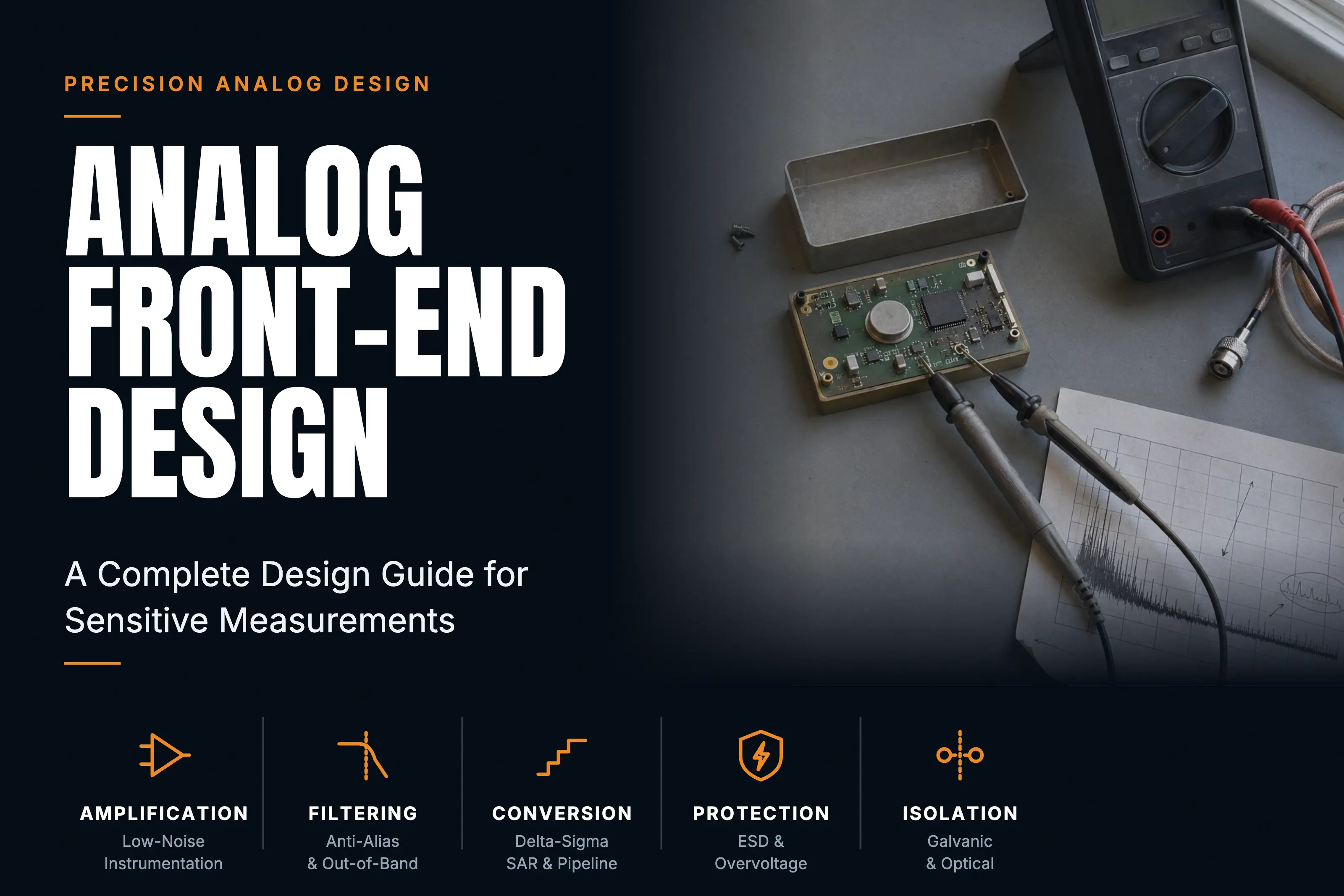
Analog front-end design (AFE design) is the discipline of conditioning real-world signals from transducers, chemical electrodes and cells, photodiodes, and other sensors that produce analog outputs, most commonly so that they can be digitized faithfully through a process that commonly includes amplification, lowpass filtering, and analog-to-digital conversion. On rare occasions, they may also undergo purely analog processing to produce an equally analog output, in which case they must be analyzed for such things as system stability, phasing, undershoot, overshoot, and general system responsiveness. They are engineered as a chain with a noise budget and circuit protection requirements.
Regrettably, it’s also an older player’s game, and as such, the skills to play it are what modern electronics teams with younger members most likely lack. The industry spent twenty years training software and digital engineers. Engineering schools, recognizing that they attract students in part by advertising high starting salaries upon graduation, found it far easier (and more financially advantageous) to mint graduates with entry-level digital and computer skills than magically to replace the many years of experience one needs to accrue to do analog design well. And tinkering in the basement was an activity that slowly disappeared from childhood experience. The future “analog guy” in 1973 was the eight-year-old kid who built a crystal radio in his Cub Scout troop, got hooked by the experience, and spent the next ten years before going to university taking his lawn-mowing and snow-shoveling money to the local electronics store for components. By 1990, the local Radio Shack had cleared its shelves of small electronic parts and was only selling cell phones and handheld electronic games. And an entire generation of potential analog circuit designers got skipped over in the process.
Today, the people who can design a low-noise instrumentation amplifier have mostly retired or become very expensive to hire. The unemployment rate for people with these skills typically hangs at about negative six percent. Companies get these kinds of people by poaching them from other companies with lures of higher salaries, sign-on bonuses, and extra job perks.
Or they come to Focus Embedded to rent them for a very reasonable price for the period over which their skills are needed.
Everyone knows how to blink an LED. Fewer and fewer know why their 24-bit ADC returns only 14 usable bits. And although a bit of clever averaging might resolve just one more bit, it won’t get you the half dozen or more bits underneath it if the data were badly corrupted to start with.
This article explains what a real AFE involves, where measurement products actually lose their accuracy, and how to scope out analog work honestly - before the firmware team is asked to trade bandwidth for accuracy in order to average their way out of a hardware problem.
Analog front-end design - key takeaways
- An analog front-end is the amplify–filter–digitize chain between a sensor and the processor, and its quality decides the limits of your product's measurement performance. No firmware can add information that the AFE destroyed. In many cases, it also needs to include protection circuits that cannot affect the signal being measured and will have to be of high enough impedance not to disturb the signal source itself with excessive loading. Biological signals can be tricky to measure precisely because what’s at the other end of one might be sufficiently adaptable as to change its behavior completely in response to seeing your electronics attached to it. The most advanced machines of today aren’t quite as sophisticated as a single cell, but to be fair, Mother Nature got about a 3.8 billion-year head start.
- Design starts with a noise budget. Every stage's contribution is calculated to ensure that the system can meet the resolution the spec promises without dipping below the noise floor. If nobody on the project has done that math, specifications become little more than wish lists.
- ADC resolution is frequently a marketing number. At most, it is an enticement for a good designer to give the part’s datasheet a closer look, not to design it into any system automatically. Effective resolution after real noise, drift, and layout can be lower, and the datasheet's conditions are not your product's conditions. Resolution in and of itself isn’t the be-all and end-all spec, either. A few missing codes or nonlinear regions in an ADC’s response can negate all of the virtues of a high-resolution converter.
- The four accuracy killers are noise, offset/drift, layout, and grounding - three of the four can be set by either good or poor PCB design, not the schematic.
- Oversampling and filtering in firmware trade bandwidth for resolution and can't remove either correlated interference or some high-frequency component that, thanks to undersampling, got folded back down into the portion of the frequency spectrum of interest. Some unyielding mathematical limits set by Messrs. Fourier, Shannon, and Nyquist will often determine the limits of what you can remove from a noisy signal in software.
- SPICE is a wonderful tool, but it pays to validate a design with measurements, not simulations alone. Noise floor, ENOB, and drift should be measured on real boards across ambient temperatures (and, depending on the signal being measured, humidities). A SPICE analysis and actual testing go hand in hand, and the results of one should agree with the results of the other. Certainly, the prototype needs to be run thoroughly through its paces before any volume order of production PCB’s, and building small “test boards” with key circuit elements on them even before the prototype board is built can often address questions of how a signal should be run, where a guard ring should be placed, how an analog ground should be poured, and how it should be separated from its digital counterpart. None of this is engineering that should be attempted after the fact. This is critical work that needs to be done up front.
What an analog front-end actually contains
Every measurement chain must address the same five requirements:
Amplification: Often, we need to raise microvolt signals to where they neatly fit the ADC's input range without adding noise or system instability. The first stage dominates: its noise is amplified by every stage after it, which is why the input amplifier is chosen with great care. In the process, at a minimum, we have to review input noise, bias currents, source impedances, and common-mode rejection ratios for differential sensors. The output of the sensor may be of comparatively high impedance, meaning that it could be easily loaded and distorted by any amplifier input stage that itself isn’t high impedance. Once a signal is past the first stage, since usually that first amplifier has a relatively low output impedance, signal loading becomes far less of an issue. But where the analog circuits first touch the sensor, it pays to be cautious.
Analog Filtering: There’s no point in measuring parts of the frequency spectrum where the signal simply does not reside. All that does is add the noise floor under a frequency band not of any interest. A good analog front-end filter rejects out-of-band interference. Critically, a well-designed AFE knocks out any higher frequencies that might alias down into the signal’s frequency band of interest before conversion. True, some demodulators intentionally undersample signals of interest to get them down to baseband. But this is not something you want to do unintentionally. And aliasing is irreversible: once 250 kHz switcher noise folds into your 10 Hz signal band, no algorithm ever separates them again. At the same time, going overboard and setting too low a filter break point or choosing the wrong filter circuit topology with the wrong number of poles can seriously distort the signal’s phase.
Conversion: The ADC architecture needs to be selected for a wide variety of factors including (but not limited to) conversion speed and accuracy. Delta-sigma converters can deliver a highly precise signal, but at the cost of speed as bit resolutions increase. The old standby SAR DAC achieves moderate speed and moderate precision that are often perfectly adequate for a wide variety of signal processing jobs. A flash converter is built for speed (and correspondingly high power consumption), but these tend to be more expensive as a rule and are frequently less precise. And there are quite a few other architectures that combine pieces of one or more converters. (The “half flash” converter comes to mind.) ADC’s can use pipelining for throughput, but usually at the cost of the very first conversion being slower than the rest and of a certain amount of latency throughout the data stream. Pipelined ADC’s lend themselves well to video systems, where frame rates may be in the double-digit Hertz but bit times may be well down into the nanoseconds. (Pipelined ADC’s are often seen in medical imaging systems that may be taking just a single still image for a function such as tomography.) Still, all ADC’s depend on their reference quality and the cleanliness of their power supply. And a voltage reference (assuming the ADC doesn’t have its own internal laser-trimmed diode reference) is the benchmark against which every measurement is made. A cheap reference with 50 ppm/°C drift can turn a good 24-bit converter into a poor thermometer.
Protection: This is what assures that your AFE and ADC survive the real world, which comes with ESD, overvoltage, reversed leads, or a visit from the engineering intern armed with the wrong tools and a bit too much enthusiasm. Protection devices leak and add capacitance, however, so even this "simple" stage has to be taken into account in any signal/noise budgeting. Additionally, the physical positions of these devices on a PCB need to be considered in manufacturing, since protection diodes are usually best placed close to a potentially unruly source. As a consequence, they frequently come in very small passive packages. (0201 SMD’s are common for ESD protection diodes). Since many signals to be measured come into the PCB via connectors (which can be quite a bit physically larger than an 0201 diode), there’s naturally bound to be a PCB line-width mismatch somewhere as a signal gets “necked down” in copper. This often has to be taken into account. Additionally, putting large connectors near small diodes has to be considered carefully if the connectors are SMT devices that might “shadow” the soldering of the smaller diodes when sent through a solder reflow oven. This is less critical if the connector is through-hole, as the protection circuits are usually soldered to the PCB in an SMT reflow oven with the connector uninstalled, which means there is no large component to cast an infrared shadow. The connector is then installed in a later wave-soldering (or even hand-soldering) step.
Isolation (when needed): Occasionally, there needs to be some optical or galvanic separation for a patient connected to a medical device, industrial field wiring, or anything sharing signals with things that spark. Additionally, with sensors that are remote, there can arise the question of whether a local ground is the same ground as a remote one. All of this has to be considered when AFE and ADC circuits are designed. Fixing a safety problem or eliminating a buzz after the fact puts you in redesign territory.
IMPORTANT: The AFE is a chain, and its performance is set by its weakest link - but its cost is set by the strongest. A common failure mode in review is a $12 precision ADC fed by a $0.30 op-amp through an unfiltered trace: the money was spent where the datasheet was most impressive, not where the noise budget said.
Where measurements actually go wrong
1. Nobody did the noise budget
Mistake: Parts are chosen by a datasheet headline ("24-bit!", "low noise!") or input from an AI tool without anyone summing the more deleterious contributions of the AFE so that they can be compared against the required resolution. Consequence: the prototype reads plausibly but noisily; the team discovers at validation that the spec was never achievable. Fix: an hour of arithmetic - source impedance, amplifier noise, resistor Johnson noise, reference drift, ADC ENOB - before the first part is placed on a schematic. This is exactly the "hard math early" that separates measurement products that ship from ones that get respecified. If one wants to be particularly cautious – and we regularly recommend this approach with things such as extremely low-level biological signals where getting buried under the noise floor is quite easy – one can build a small test PCB to make sure that grounds are where they need to be, sensitive signals are protected from environmental noise, guard rings are in place if they’re required, etc.
2. The layout undid the schematic
Mistakes: A properly done schematic with correct circuit topologies and properly chosen component values gets routed as if it were a digital board - analog traces through the switcher's neighborhood, ground "handled" by a single shared pour, reference traces treated like any other net. Consequence: performance far worse than simulation; Problems are intermittent, temperature-dependent, and downright maddening. Fix: analog layout discipline: physical separation of noisy and quiet domains, star or carefully partitioned grounding, guarded high-impedance nodes, Kelvin connections for current sensing. On mixed-signal boards this is where analog design and PCB layout must be parts of the same conversation.
3. "We'll fix it in software"
Mistake: treating firmware averaging as a substitute for analog engineering. Consequence: oversampling buys resolution only against uncorrelated noise, and each doubling of samples buys at best only half a bit while being guaranteed to halve your bandwidth. Against correlated interference - switcher harmonics, 60 Hz pickup, etc. - averaging buys approximately nothing. Fix: software filtering as the last stage of a designed chain, with the analog work done first. Done in that order, digital filtering is genuinely powerful. But when to use analog filtering (and which topology of active filter to use) and when to use digital filtering (and whether to use FIR or IIR math) are most definitely decisions to be made when doing system architecture.)
4. Validation by demo
Mistake: "It reads correctly on the bench" is accepted as validation. Consequences: drift from temperature changes and other variations in ambient conditions end up surfacing in the field, one RMA at a time. Fix: Measure the noise floor with the signal input suppressed, measure ENOB with a precision source, run temperature sweeps, and log your results for days – on multiple boards – during the prototyping phase. The difference between a measurement product and a demo is the data proving it. And “shake and bake” labs do brisk business for a reason.
Choosing the ADC (and believing the datasheet correctly)
The datasheet number that matters is rarely the headline resolution. Read instead:
What the datasheet saysWhat to check"24-bit ADC"Noise-free bits / effective resolution at your data rate and gain - typically 18–21 bits for a good delta-sigma, and that's under ideal laboratory “evaluation-board” conditions"1 MSPS"Whether any multiplexing, settling, and drive amplifier let you use that rate at rated accuracy. It pays to be aware when and how the sampling window opens and, if a converter is pipelined, how it gets itself prepared for the sample coming in behind the current one."Internal reference"The temperature coefficient (ppm/°C) of your reference needs to be checked against your temperature range and accuracy spec. And it’s worth remembering that internal references are often conveniences, not precision instruments. Furthermore, noise on a reference ends up as noise on a signal, often at greater amplitude."Rail-to-rail input"Nothing advertised as “rail to rail” ever truly is, although some parts are mighty close. Still, a little safety margin never hurts. Often, any small reduction in amplitude of an input signal can easily be made up at a place where it’s a lot safer to do so than in a place where trying to operate all the way to Vcc or Ground is going to add tiny bits of either distortion or (worse) clipping.Evaluation board resultsThe layout, supply, and clocking of that eval board are often optimized to show an amplifier or ADC to its best advantage. Your product ideally should have most of the PCB features presented by these exceedingly useful cards, but often you’re threading a needle so that some other unrelated circuits on the same PCB have the space or layer stackup they need. Ultimately, reality is all about tradeoffs. Fortunately, reputable silicon manufacturers such as TI and Analog Devices will document the gap between their ideal and a few real-world situations sufficiently honestly that you can do some intelligent planning. But not everybody does this, and it pays to be aware.
Architecture selection is usually straightforward once the noise budget exists: delta-sigma for slow precision (weigh scales, thermocouples, bio-signals), SAR for mid-speed multiplexed acquisition (control loops, industrial monitoring), pipeline/RF-sampling when bandwidth (video systems, software-defined radios, etc.) is the product.
Scoping and budgeting AFE work
Precision analog is specialist work with a shrinking talent pool, and the market prices it accordingly. But it's a bounded, front-loaded cost. Prices for for design plus validation of a precision channel are driven by:
- Required resolution and bandwidth. (Each decade of dynamic range adds to the challenge).
- The environment (benchtop vs. industrial vs. patient-connected - isolation and standards add scope).
- How exotic the sensor is. (A thermistor is a solved problem; a pH electrode at 10¹² Ω source impedance is not.)
- How much validation the claims on chip datasheets require.
Questions that separate real analog capability from optimism, in a vendor conversation or an internal review:
- "Show me the noise budget." (Numerically, please…)
- "What's the expected ENOB at the system level, and how will we measure it?"
- "Which stage dominates the noise, and what would improving it cost?"
- "How does the layout partition analog and digital domains?"
- "What's the validation plan across temperature?"
How Focus Embedded can help
Low-noise analog is one of our founding competencies - the "rare in the modern era" skill our clients most often can't hire for. We do the SPICE analysis, the noise arithmetic, and the layout discipline as one engagement.
Analog and mixed-signal design
- Sensor signal conditioning, instrumentation amplifiers, precision ADC/DAC channels
- Noise budgets and SPICE analysis before schematic capture - math first, silicon second
- Mixed-signal PCB layout with analog partitioning and grounding done by the circuit's designers
- Power supply design that measurement channels can live next to
- See our analog hardware design services →
Why work with us:
- ✅ We have a history of shipping precision systems with analog front ends, including a pressure transducer amplifier and instrumentation for light aircraft, where a bad reading isn't a bug report - it's an incident
- ✅ We also have analog, digital, firmware, and layout in one team: the noise budget survives from schematic to copper
- ✅ We also do honest scoping of your project. If your accuracy spec is achievable with a $4 integrated AFE chip, we'll point at it. We’d rather send you away with less engineering time burnt if there’s an easier way to do things. But knowing that there is one and that it’s not a cheap “cheat code” that will come back to haunt is where the skill (built by decades of experience) lies.
Ready to hit the accuracy your spec promises?
Talk to an engineer, not a salesperson. Send us the sensor, the resolution target, and the environment - we'll tell you what the physics says it takes.
📞 +1 (512) 246-9012 (or 1-888-FOC-7924) 📧 info@focusembedded.com 🌐 focusembedded.com/contact
Summary
- The AFE sets the ceiling on measurement performance; everything downstream can only lose information.
- Start with the noise budget - an hour of arithmetic that decides whether the spec is engineering or wishful thinking.
- Layout is half the design: partition, ground, and guard, or watch a good schematic perform like a bad one.
- Software filtering is the last stage of a designed chain, not an apology for a missing one.
- Validate with measured noise floor, ENOB, and temperature data on real boards - before the volume order.
Precision isn't a component you buy. It's a budget you keep.
Related articles
- High-Speed PCB Layout: DDR, PCIe, USB & MIPI Without the Respin
- Embedded Software Development Services: What They Are (And How Not to Pick the Wrong Partner)
