PCB Interposer
Client:
A Designer of Military Avionics
Competencies:
PCB Design
Working with Manufacturer for Complex Assembly Problem
What We Do: Fix an Incorrectly Routed PCB’s
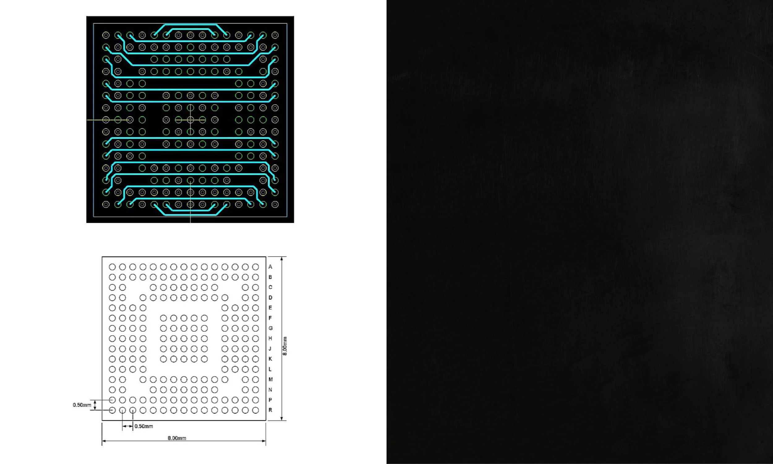
There are a lot of components on the modern PCB that aren’t standardized in terms of pin numbering. It used to be that things like connectors were all we had to worry about. But now with BGA, uBGA, and LGA parts; there’s a lot of variation out there. The result is that what may be pin A1 on one chip could be pin Z26 on another chip with a mechanically identical footprint. And it can be all too easy to miss this fact when pulling PCB footprints from a library. The result? Often it’s a PCB that cannot possibly run at all.
Our job is to figure out how to build small PCB’s (“Interposers”) that can be sandwiched between the incorrect footprint on a PCB and the bottom of a chip. This is never an ideal solution, and it’s generally not something anyone would ever put into production. And often the limitations of routing the interposer (and the degree to which the PCB footprint is in error) are such that it can only unscramble a subset of all pins that are in the wrong places. But often getting just a subset of pins routed can get an otherwise dead chip to boot and a project from being completely stalled.
There are tricks and techniques we use (in concert with our manufacturing partners) to uninstall your BGA/LGA from the bad footprint, and put it back down on a board that may get a lot (if not all) of the problems unscrambled so that time and money isn’t completely wasted.
How We Do It:
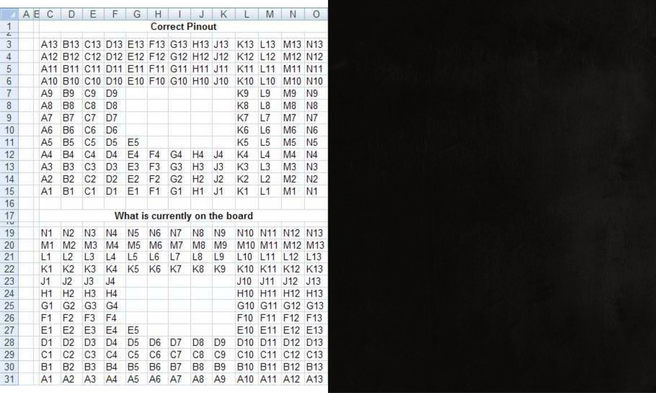
Typically when a PCB layout gets screwed up, the problem is that somebody lost track of the ordering of pins on a large BGA chip. And as crude as it may seem, often our starting point is a spreadsheet that outlines what’s on the board now and how we want things to be eventually. Based on that, we can start to identify what the important signals may be and how best to route them first.
The reality is that when a large device (particularly a uBGA) footprint gets scrambled to the point where hand rework is no longer a solution, it may not be physically possible given mechanical constraints to devise an interposer card that can correct it all. There are just too many signals in too dense an area that need to be swapped, and no number of layers of PCB would allow it because of the staggering number of vias that would be required.
Nine times out of ten what a failed first prototype board does that is most damaging to a development schedule is that it blocks further code writing, since there’s no working target hardware on which to run firmware or test HDL code. Unblocking this can keep the overall project moving forward while a replacement prototype board is laid out. So we work with customers to make the trade-offs that allow them to get the bad board working well enough to facilitate the rest of their development effort, which would otherwise be dead in the water.
Each of these interposers is done on a case-by-case basis, and since creating one requires some understanding of the PCB on which it will go, the process is far from rote. But done correctly, it can rescue a project and prevent months of development delays.

Step one of doing an interposer is building the spreadsheet that shows where you are and where you need to go.
How We Do It:
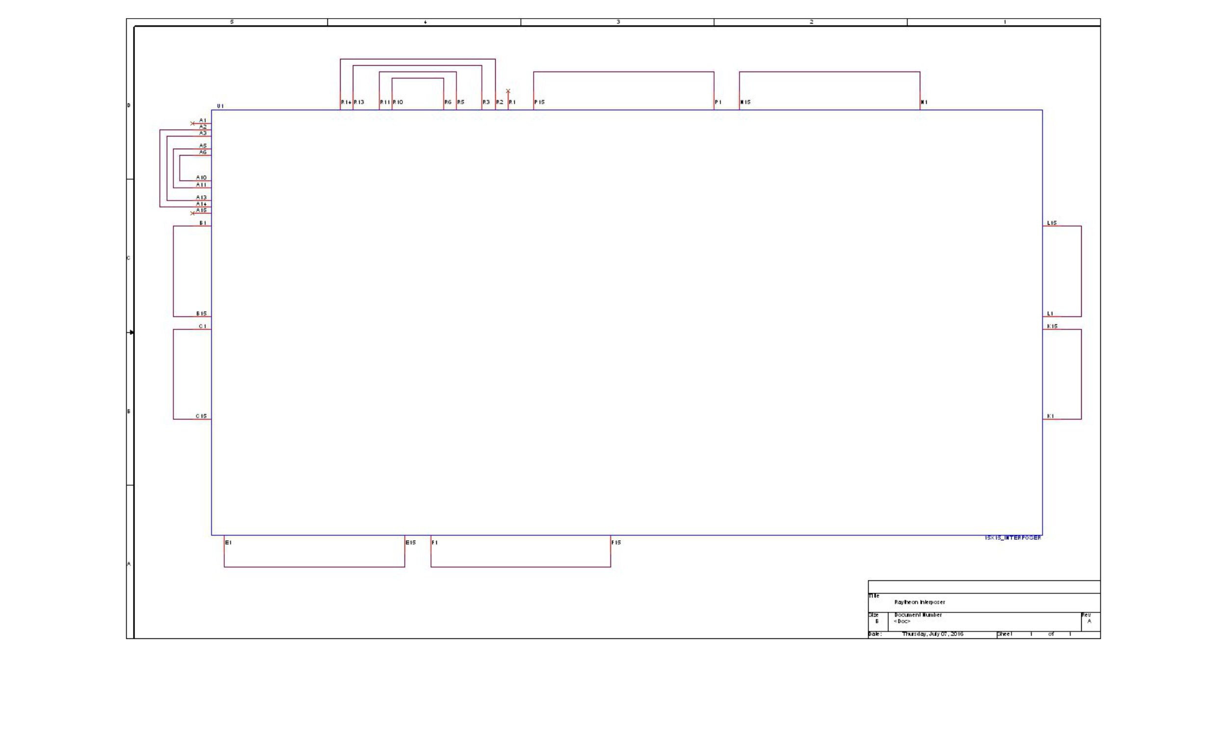
Armed with a spreadsheet of what matters, we can create a basic schematic that exchanges pins. Such a schematic usually contains two elements: The “wrong” footprinted device and the “right” one. Occasionally, we also migrate critical components off the main PCB onto the interposer as well, such as the requirements of the overall design dictate.
(A common example is migrating a crystal and the pair of capacitors that go with off the main PCB to the interposer. We do this to assure that a Pierce oscillator inside the BGA chip will fire.)
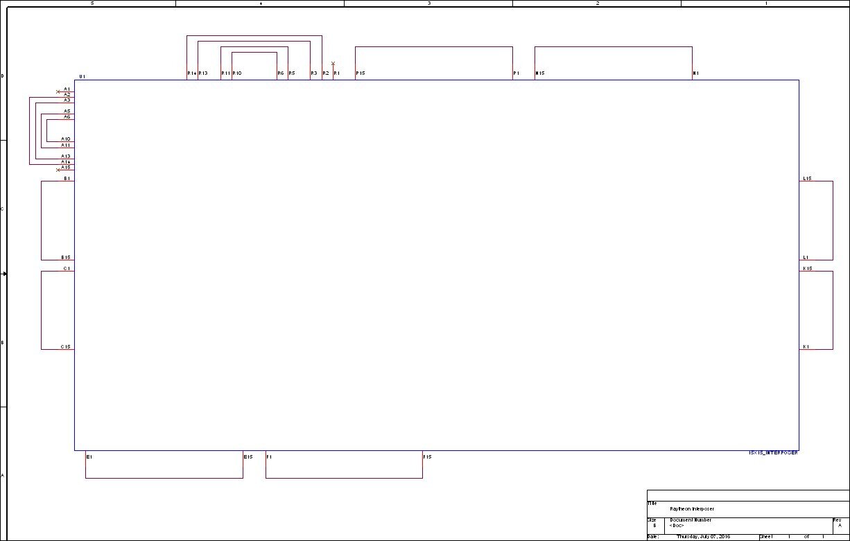
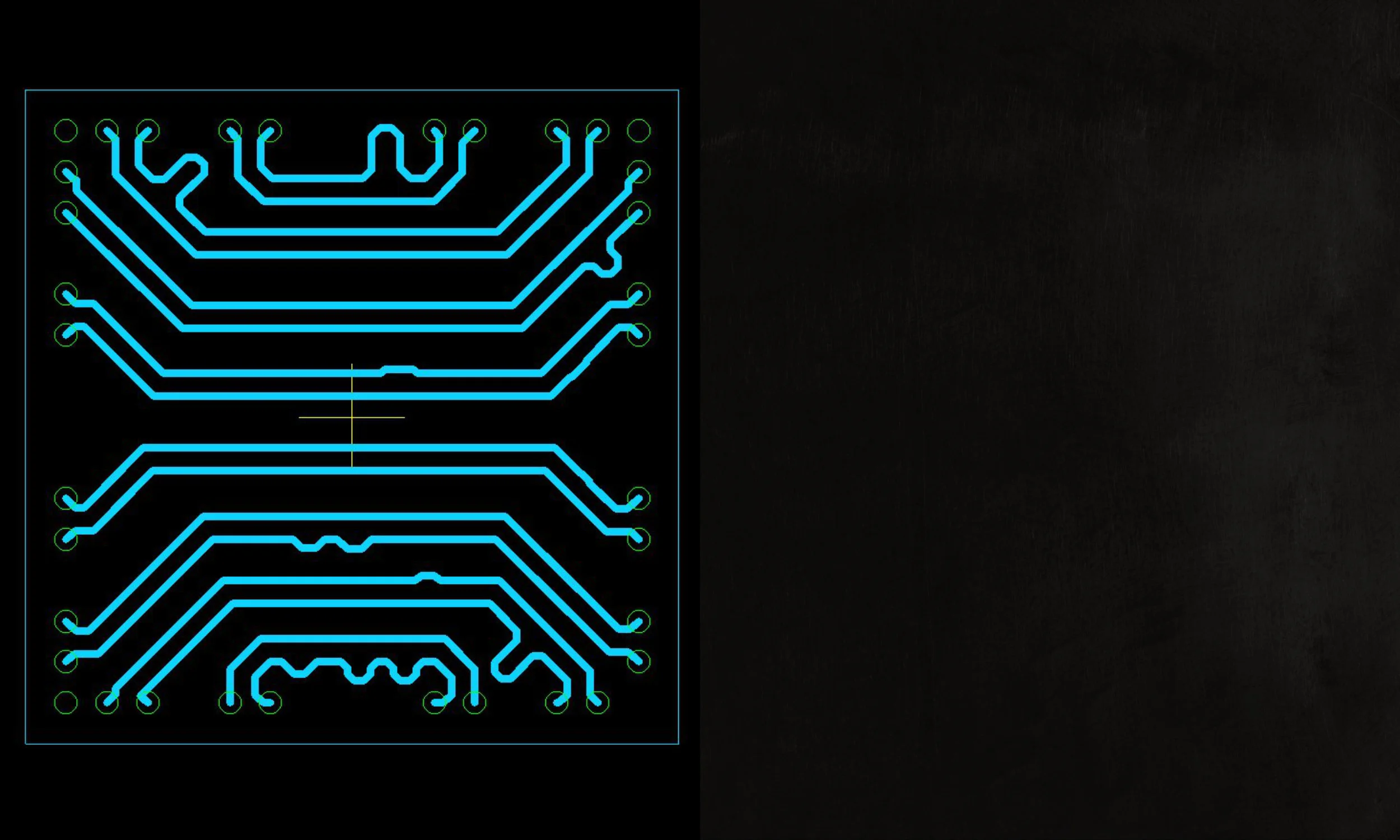
The stripped down uBGA footprint as shown in schematic capture, with the wires that need swapping appropriately connected to each other.
The Project: A Simple Interposer
Sometimes we get lucky and a single, simple reroute will untangle things. At right is an example of a uBGA chip where the footprint on the actual PCB had rows numbered 1-15 when they should have been numbered 15-1. And enough of the rest of the pins were either “no connects” or went symmetrically into a power or ground plane that there was nothing to route.
Not all interposers are this easy, but when they are, we can usually spot them and make fast work of them.
