
Picking the wrong compute architecture is among the most expensive mistakes a development team can make early on a hardware project, and it’s an easy mistake to make, even before anyone has written a single line of code.
This guide is for the system architect deciding what to platform on which to build, not the engineers who will eventually design the circuit topologies at the component level or write the firmware. It explains, in plain language, what an MCU, an SoC, and an FPGA (or CPLD) actually are, when each one is the right call, what each one really costs, and where this decision quietly sinks products. If your team is already arguing about individual component values and programmable logic cell counts, send this to whoever is signing the checks first.
Technical summary (the short version)
Here are a few of the major options available to the modern hardware designer:
- MCU (microcontroller): In the modern world, this is usually a single chip with a CPU, memory, and a few useful peripherals (a counter-timer or two, a UART or serial communications controller, and maybe a 10-bit or 12-bit ADC) baked in.
If a microcontroller can do the job, it usually pays to use one. Often it pairs well with a small FPGA, which can handle the most hardware-intensive functions while being run as a slave to a microcontroller host. A handful of microcontrollers (such as the Cypress/Infineon “PSoC” families of parts) contain dedicated programmable logic fabric (similar to that found in an FPGA), allowing users to enjoy the best of both worlds.
- FPGA: A chip full of unallocated logic you wire up yourself, usually using a specialized hardware description language (HDL) such as VHDL or Verilog – or on rarer occasions, using hardware schematic diagrams. Some FPGA tools, such as Xilinx’s “Vivado,” allow mixed-mode (schematic and HDL) design, and often within these environments, a schematic block diagram will outline the overall structure of a design while the contents of the blocks will be defined by an HDL. An FPGA is designed for speed, since what is in it is purely a piece of hardware that doesn’t have to fetch an instruction from memory or spend multiple clock cycles decoding what it should do with whatever instruction it just fetched. It is hardware that simply runs in place at full speed. You don’t code for it as much as you design its hardware yourself using the blank silicon tablet the chip provides.
An FPGA is usually the choice when timing is tight and unforgiving, throughput is enormous, or no off-the-shelf part does what you need. It can have higher unit cost and almost always comes with the highest engineering cost due to how few people can design them well (and how expensive hiring a good designer can be). But in some situations where speed is everything, it’s the only thing that works.
- SoC (system-on-chip). This is perhaps the least precise of all technical terms, since what constitutes a “system” and what is a “chip” can vary depending on situation and interpretation. Still, it’s safe to say that in most situations an SOC is a complicated processing engine with most (if not all) of the trimmings and that it sits closer to the end of the embedded spectrum labeled “single board computer” than does a microcontroller, which usuall has less memory and fewer peripherals. An SoC is also usually quite a bit less flexible down at the hardware layer, since when so much is provided to you in peripherals (and their associated drivers), you don’t get to make nearly as many of your own choices about what gets wired to what or how some lower-level application programming interface (API) is structured.
A more complex SoC can be a good choice if you’re going to drive a screen, a network stack, or a complex filesystem – or you just need a great deal of computational horsepower. SOC’s generally come with higher unit cost and higher complexity, but they can also shorten some of the development time if there’s an off-the-shelf, open source driver that does something that’s not a part of your company’s “secret sauce.”
With so much of the world being part of an “internet of things,” SoC have become popular if only because they can run some variant of Linux that has a robust Ethernet protocol stack built into it.
- A good rule for navigating the embedded food chain: Start by assuming an MCU. Move up to an SoC only when software requirements force it. Reach for an FPGA only when the physics of the problem - latency, determinism, or raw parallel throughput - leaves you no other option.
Note that the selection process is driven from the top down: The questions to answer in order are, “What are we trying to achieve?” then “Do we need hardware to meet a timing objective?” and then, “How much processor is required to run the code we need to run?”
- The honest caveat. Many serious products use two of these together (for example, an SoC with an FPGA fabric on the same die, or an MCU paired with a small FPGA). And more than one motion control system (3D printer, CNC milling machine, industrial robot, etc.) has an SoC on top to get Internet connectivity, some embedded microcontroller below that to run a Real-Time Operating System (RTOS) to synchronize motors, and an FPGA below that to handle things like generating the pulse-width modulation signals going to motor windings. Using one technology hardly precludes using the other two, and a great deal of good system architecture design lies in figuring out just what tasks are best done by what.
Herein, we present the rest of this article, which is the long version - including the numbers most vendors will not put in writing.
Why this is the decision that haunts you
Many of the lower-level choices you make on an electronic hardware project are reversible without major overhaul of the design, and it’s common for a complex product to undergo as many as three to five prototype iterations as all of the minor bugs get chased out. On the mechanical side, a bad enclosure can be redesigned. In the realm of software – where design is as malleable as it gets – an awkward menu can be reworked or a clumsy (or even unreliable) driver can be rewritten so long as the change doesn’t force some modification of the hardware.
The overall architecture of a system is generally not like that, as it is integral to almost every other part of it. The uppermost block diagram defines everything logically instantiated below it, and everything else is built to suit the implicit assumptions it encapsulates. These include your hardware peripherals, your power budget, eventually your board layout, your firmware, your bill of materials, your certification path (UL, CSA, EU, FCC, etc.), and even how easy your product is to manufacture. It also drives your design tool and IDE selections, and coming up the learning curve on a tool (or purchasing one, if it’s not supplied for free to encourage use of its target chip) can easily be another major investment of time and money. Change the architecture late, and you are not editing a few rough spots out of a good first draft of a novel - you are starting over and most likely telling an entirely different story.
This is the lesson to which we keep coming back: most failed projects were doomed sometime during the first week, when somebody defined the problem incorrectly - or, just as often, picked the wrong foundational technology on which to build it. The really hard problems get solved with old-school math and science first and newfangled silicon second. Choosing your processor before you fully understand the subtleties of your problem is how good teams end up having to perform minor miracles such as shoehorning a jitter-sensitive data-taking subsystem into a microcontroller that never had the timers to run it or implementing a digital filter in a processor that wasn’t set up for repetitive multiplication and accumulation.
So before you fall in love with a chip, get clear on what the three families actually are.
The three families, in plain language
Microcontroller (MCU)
A microcontroller is an entire small computer on one chip: a CPU, some RAM and flash, and a fistful of peripherals - timers, ADCs, UARTs, SPI, I2C, PWM, etc. A microcontroller design is often the cheapest embedded control, measurement, or instrumentation option. It is also the most straightforward to develop, and it is most suitable for simpler applications where speed of execution and timing latency are least critical. It’s the default (and usually correct) choice for most relatively simple products.
Almost half a century ago, early microcontrollers such as the Intel 8051 relied on external memory. Perhaps if you were lucky, back in 1980, you got a low-speed UART and a little one-time programmable (OTP) ROM built into the chip itself. Well into the 1990’s, there remained a market niche for silicon makers such as Waferscale Integration to produce everything microcontrollers of the day were missing, calling them “Programmable System Devices.” (Usually these included an address decoder, some program ROM, some scratch RAM, and perhaps a watchdog timer.) Today’s microcontrollers from one vendor or another are often grouped in families, and within any family one can choose a variant that has the peripherals and memory required for a specific task. Having at least some ROM and RAM internal to the processor is a given in the modern world.
Today, modern ARM architectures are becoming common across multiple vendors. Largely gone are the days when semiconductor manufacturers would design their own embedded processors and build their own development tools around them. Since the early 1990s, when it began life as a small company backed by Acorn Computers, Apple, and VLSI Technology, the multi-billion dollar technology giant that is ARM Holdings, PLC (Cambridge, UK) has been creating variants of processors that can be sold in “soft” (physically unimplemented) form to semiconductor makers as intellectual property they can reduce to semiconductor mask sets when they put them in their chips. Concurrently, the GNU community has developed compilers, debuggers, and libraries for these “ARM cores.” Most modern makers of embedded microcontroller chips have long since abandoned further development of their own in-house architectures, and if proprietary architectures exist in the market at all today, it’s because they’re supporting legacy products and systems.
True, it seems that the x86 architecture will be with us all forever, and there remains just a bit of development on it, even as Intel and AMD direct more and more of their resources to developing chips for the desktop, not the embedded space. But slowly, other processor cores like the aforementioned 8051 and the Microchip PIC lurch towards extinction after decades-long (and in most cases, profitable) runs. Many of them blazed new trails decades ago, and the modern world wouldn’t look as it does had they not done so. But ARM and its “Cortex” variants currently appear to be the wave of the future, particularly because their current consumption is quite low and thus well-suited for battery-powered applications.
The obvious benefit to this kind of processor core standardization is that the developer of microcontroller systems doesn’t need to select a particular chip vendor or tool suite until far later in the development process. He can write C code for the ARM system closest to hand and decide on a final hardware target once he’s more confident what he actually needs as far as processor speed, memory configuration, peripheral set, etc.
You write firmware, the microcontroller runs that firmware, and in combination that hardware and the algorithm running on it define the product. Think ARM Cortex-M parts from STMicroelectronics, NXP, TI, Nordic, or Infineon.
Also, moving memory inside the chip itself – and encrypting its contents or blocking it from being read externally after it is programmed – became increasingly important as software piracy and intellectual property theft became more prevalent throughout the 1990s and 2000s. Having a memory area into which you can pour code so the processor can read it but it can’t be read back out by anything else has kept many a company from being the victim of piracy.
Finally, at the lower end of the spectrum as far as task complexity and unit cost are concerned, there’s a gray area where the functionalities of FPGA’s and MCU’s cross over. Usually, because more people can write C code than can design algorithmic state machines using a hardware description language (HDL) for an FPGA, the MCU gets chosen as the solution if it’s a toss-up. The overall labor shortage for FPGA designers simply biases the development in favor of the microcontroller.
To sum up, microcontroller tools are mature, the community that supports them is enormous, economies of scale keep their per-chip costs low, and a competent firmware engineer can usually have one blinking lights and talking to sensors in just a few hours. For the overwhelming majority of embedded products - sensors, controllers, wearables, simple connected devices - a microcontroller-based circuit board is not a compromise. It is the correct answer.
System-on-chip (SoC)
An SoC is what you graduate to when an MCU runs out of room. It is typically a more powerful processor - often multi-core, frequently Cortex-A class - with memory controllers, high-speed interfaces, a GPU or video engine, and enough muscle to run a full operating system such as Windows, embedded Linux, Android, or iOS (the latter three of which all have UNIX as a common ancestor).
A “chip” in this context, for example, may be a traditional piece of silicon in a plastic package, but it can also be two or more such chips on a single module that is treated as if it were all one device.) An SoC may boast a more powerful processor (often multi-core, and frequently ARM Cortex-A class) with rich peripherals, capable of running a more complex operating system (frequently an RTOS if hard real-time performance is required and embedded Linux if it isn’t).
An SoC may also be like the classic “BeagleBoard” processor, the Texas Instruments “OMAP 3530,” in which an ARM processor shared space with a functionally dissimilar TMS320 DSP inside the same package. Such a chip may itself have solder pads on both top and bottom sides so that the chip can be soldered on a PCB at the same time that a memory chip can be soldered on top of it.
And an SoC can be like the Cypress/Infineon “PSoC” families of processors, which have Cortex-A or Cortex-M cores on a single piece of silicon that also contains some blank programmable logic that awaits programming. A PSoC (or its equivalent) is likely the chip to use when you need just a small bit of very fast logic to supplement what is being done by a processor core and you don’t want to increase BOM cost by adding a small FPGA or CPLD.
In the end, you reach for an SoC when your product needs a real screen, a real network stack, a filesystem, a camera pipeline, or computational power that an MCU simply cannot deliver. The price you pay is complexity: SoCs almost always need external DDR memory, more complex power management (possibly to include startup sequencing), a more demanding PCB layout (and likely a more expensive impedance-controlled board) that includes high-speed routing, and a non-trivial board support package to supply even the most basic functionality. More power, more parts, more expensive parts, and often more bring-up.
FPGA (and its smaller cousin, the CPLD)
A field-programmable gate array is a different animal entirely. It is not a processor running your code instruction by instruction. It is a sea of logic blocks and interconnects that you configure with hardware description language to be the exact digital circuit that solving your problem demands. When someone asks which line of your FPGA design’s code is "running," the honest answer is: all of them, all at once.
Here is where an FPGA becomes difficult to program as compared to a microcontroller. Because all connected registers (single bits of memory) are designed to be loaded simultaneously with whatever logic also internal to the chip sends their way (usually either a “one” or a “zero” to be written into just that bit) with every clock cycle, the entire logical contents of all FPGA registers (all those single bits) can theoretically change instantaneously. This allows a designer to create a system capable of doing many things truly in parallel. But it also means that a designer has to be aware of every state a system in which a system could find itself – and every future state into which it could go. One way of thinking about this structure, as compared to a microcontroller (which executes one line of code and then moves on to execute the next line of code), is that an FPGA effectively executes every single line of code all at once, pauses for the next clock cycle, and then executes every single line of code again. That parallelism is the whole point. An FPGA can ingest a firehose of data and process it in real time, with deterministic, nanosecond-level timing in ways no sequential CPU can match.
The big three vendors today are Xilinx (now AMD), Altera (now Intel), and Lattice Semiconductor, and each has carved out its section of a sprawling marketplace. Xilinx and Altera have focused primarily on the very highest performance niches in the market, often where cost of a chip is a secondary concern and the high quality of peripherals in and FPGA chip can justify its cost. Consider, for example, the FPGA in a cell phone tower, where millions of conversations are being passed about at once and vast data pipelines are constantly flowing. Chips that implement those data-moving functions are often sold not just on the quality of their internal logic but also on the quality of the SERDES that resides with it. And a single FPGA to go in a cellular tower can easily cost $30,000. Economies of scale make this possible, as even a relatively local cellular network can be carrying millions of subscribers whose monthly bills pay for the purchase of the equipment.
Lattice Semiconductor plays at the other end of the market, where the BOM cost of the device in which their chips are installed is extremely important. On the surface, one might conclude that their chips are somehow “less advanced” than those of AMD or Intel. In reality, their design is advanced along a different axis – that of money that can’t be amortized nearly so easily across millions of users. Lattice’s chips find their way into the cell phones themselves, and in the modern economy these devices are essentially consumable items designed to entice users to select a particular cellular subscription plan or make use of a particular flavor of applications (iOS or Android), where the companies running the “App Stores” are collecting residual income from their sales. A Lattice FPGA keeps a different kind of money pipeline open.
Focus Embedded is, by the way, a factory-authorized "Leader" design center for Lattice. And this has a great deal to do with our customers being more sensitive to unit cost and less able to amortize an expensive device across millions of individual sales. The one exception to this is in the arena of medical imaging, and when we do go there, because we’re not exclusively bound to Lattice, we may find ourselves using an Intel or AMD chip in order to exploit its SERDES technology for serializing and transmitting vast amounts of image data.
A CPLD is the FPGA's smaller (and usually cheaper) sibling with less logic and a different internal structure. Whereas the FPGA has a small amount of logic attached to a D-flop or two found in the center of the part, a CPLD has D-flops positioned around the periphery of a large programmable AND-OR product term array. (The first common “Programmable Array Logic” or “PAL” chips introduced by Monolithic Memories in 1978, were structured this way.) FPGA’s didn’t really come into their own until the middle to late 1990’s, so for a time, CPLD’s (the most direct descendants of the old PAL’s) ruled the roost based on cost and speed. Since then, they’ve seen declining market share, but they’re not to be counted out for certain high-speed logic applications that don’t require the vast resources of an FPGA.
Notably, because the combinatorial logic of a CLPD is in its center and because a CPLD typically has fewer flops in it than an equivalent FPGA, it’s more common to use binary-encoded state machine design techniques, where states are generally given a unique multi-bit state code and state codes are chosen so as to minimize bit changes from one state to the next. Large sections of CPLD’s will often have state transitions that follow Gray coding. The reason for this is that if outputs are a function of state values, if more than one bit transitions, it’s possible to generate a glitch on combinatorial logic outputs when moving from one state to the next. By contrast, because the D-flops in an FPGA are more evenly spread throughout the device, and because there are more D-flops available, FPGA state machines are typically “one hot” encoded, which nearly always automatically eliminates the possibility of output glitching. In any case, the source code for the same function will be different if the target chip is a CPLD, not an FPGA, for the reason that ASM’s will have fewer state bits but more complex encoding. And a designer must be aware of what the eventual programmable device will be if he’s to write his code to make it compile optimally for the chip he’s using.
Herein lies another reason that most of the best FPGA and CPLD designers started as EE’s, not computer science majors: They’ve usually built a few ASM’s in some undergraduate lab exercise using only 74xx-series discrete gates and flops, so they’ve had to think about the hardware target from the beginning.
Historically, a formalism for making “hardware algorithmic state machines” of the kind you’ll find in an FPGA (which we’ve been discussing obliquely to this point) came about in the 1960’s and 1970’s, just as simple logic gates were first getting shrunk onto single pieces of silicon. As the earliest programmable logic devices came into existence in the late 1970’s and early 1980’s, this methodology mapped to them quite nicely, and for a few brief, shining moments, a generation of future FPGA and CPLD designers was being minted. By the early to mid-1990’s, the game was changing, and the early primitive languages (ABEL, PALASM, etc.) for “hardware description” were giving way to more complex languages such as Verilog and VHDL that abstracted away a great deal of what was happening at the silicon chip level. So a slightly newer generation of designers wasn’t learning the older methodology that built fast logic systems from scratch – or at least from the most primitive gate and flip-flop chips being wired to agree with Karnaugh maps and state transition tables.
Herein lies the reason that finding an FPGA programmer can be quite a bit more difficult than finding someone who can simply write code, even if it is a hardware description language (HDL) and its syntax looks so much like Pascal (as is the case with VHDL) or C (as is the case with Verilog). It takes a special kind of brain (capable of using some rather arcane parallel design methodologies) to code for an FPGA or CPLD. Good designers typically come out of the pool of electronic hardware designers, and they comprise their own small subset of engineers in a population that is already smaller than that of computer science graduates.
Thus, there are simply fewer people who can write good FPGA code than can write good MCU code. This is something to consider if you’re designing a system or device that could be implemented either way – and which may need to be maintained in the future by some designer other than the one who’s doing the work now.
In the end, the catch of using dense programmable logic (FPGA and CPLD) is cost - in two dimensions. High-end FPGAs are expensive parts, and the engineering is specialized and scarce whether the chip is expensive or not. In some cases, designing for a more advanced FPGA is easier than designing for a less expensive commodity part, since with the lower-end part, it can take a whole lot of skill to pack it tightly and still make it run quickly.
In any case, there is a reason good FPGA designers are hard to find, and that scarcity is a real line item in your plan, not a footnote.
FPGA vs MCU vs SoC: the comparison at a glance
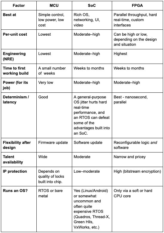
A table never decides a project, but it frames the trade you are actually making: cost and simplicity (MCU) versus capability (SoC) versus raw, deterministic parallel performance (FPGA). Most products want the cheapest box on this chart that still does the job.
When an MCU is the right call (and when it isn't)
Choose an MCU when the workload is bounded and well-understood, power and unit cost matter, and there is no need for a full operating system. Battery-powered sensors, motor controllers, instrument front-ends, most IoT endpoints, the brains inside a consumer gadget - these are MCU territory, and trying to be fancier just burns money.
It's the wrong call when you find yourself fighting the part to make it keep up: hand-tuning interrupts to fake parallelism, running out of timers, or discovering that the digital signal processing you need will never fit. We have been handed projects where a microcontroller was chosen by someone who had no idea the problem involved DSP at all, and rescuing it meant commandeering on-chip timers and aligning interrupts just to open ADC sample windows cleanly - work that a five-minute architecture conversation would have avoided. If your "simple MCU" is sprouting the kind of epicycles once used to defend Ptolemaic cosmology against the math of Copernicus, the architecture choice is trying to tell you something.
When an SoC is the right call (and when it isn't)
Choose an SoC when the product genuinely needs what an operating system provides: a graphical UI, a TCP/IP stack and Wi-Fi, a filesystem, a camera or video pipeline, or compute-heavy application code. If your software roadmap reads like it belongs on a small computer, put it on a small computer. This is also the architecture where the quality of your BSP makes or breaks the schedule - an SoC with a shaky board support package is where launches go to slip two (or more) calendar quarters.
It's the wrong call when you reached for the OS out of habit. An SoC drags in DDR memory, multi-rail power sequencing, high-speed PCB layout, thermal headaches, and a longer certification story. If a Cortex-M part with an RTOS would have done the job, the SoC just tripled your bring-up cost to run a menu. And if you need hard, deterministic real-time response, remember that a general-purpose OS introduces jitter - sometimes enough to make a control loop misbehave somewhere you weren't looking.
When an FPGA is the right call (and when it isn't)
Choose an FPGA when the physics demands it:
- Throughput no CPU can touch - high-rate signal processing, image and video pipelines, software-defined radio, high-speed data acquisition.
- Hard, deterministic timing - nanosecond-class response with no operating-system jitter, the kind robotics and motion control sometimes require.
- Interfaces nothing off-the-shelf provides - bridging exotic buses, custom high-speed protocols, or gluing incompatible chips together.
- Consolidation - folding a board full of discrete logic into one programmable part to cut BOM cost, reduce field failures, and shrink your attack surface for IP theft.
- Flexibility against obsolescence - an FPGA design can be massaged to fit a new programmable part when a chip goes end-of-life, instead of forcing a respin. (Focus Embedded did a booming busines from 2021-2024, when COVID and the constraints it placed on silicon foundries accelerated the retirement of a lot of programmble logic parts that were near EOL as it was. We put a lot of square pegs into round holes to keep people’s production lines running.)
It's the wrong call when you picked it for prestige rather than need. FPGAs carry the highest unit cost, the highest engineering cost, and the scarcest talent pool of the three. And FPGA development is unforgiving of shortcuts: in a serious effort, well over half - often two-thirds to three-quarters - of the HDL you write is testbench code that never ships, written to simulate the design exhaustively before anyone ever asks "when can we get a board?" (This is why we build testbenches and simulate across multiple engines – and avoid vendor-locked macros – before writing a line of synthesizable logic. It keeps the source portable and the bugs in their graves.
Skip that discipline and the FPGA that was supposed to save your product becomes the thing that buries it.
The honest part: you may need two of these
Real products rarely sit neatly in one column. The interesting designs combine families:
- SoC + FPGA on one die. Parts like the Xilinx Zynq and Intel/Altera SoC FPGAs put ARM cores next to programmable logic, so Linux handles the UI and networking while the fabric handles the hard real-time, high-throughput work. Increasingly common, and increasingly the right answer for sophisticated products.
- MCU + small FPGA/CPLD. A microcontroller runs the product while a modest FPGA or CPLD handles a single brutal timing or interface problem the MCU can't.
- A soft CPU inside the FPGA. Sometimes the cleanest design drops a soft-core processor (or exploits a hard core) into the FPGA, so the "processor versus logic" question dissolves into "both, on one chip." Our FPGA experience often lets us make smart calls on both sides of the FPGA-to-firmware boundary, which yields a better BSP and cleaner HDL at the same time.
The point of partitioning - deciding what runs in software, what runs in logic, and what runs in analog - is a system architecture decision, and it is the single highest-leverage time you will spend on the whole project.
What each path actually costs
Most firms won't put numbers in writing. We will, because vague pricing is how buyers get hurt. These are rough orientation ranges for a defined, single-board design at experienced North American / Western European rates - your mileage varies with peripheral count, regulatory scope, and how mature the silicon is.
Per-unit silicon (rough orientation)
- MCU: often well under $1 to a few dollars. A fancy uC can cost up to $10 in low quantities.
- SoC: Typically tens of dollars, plus the cost of any DDR and power parts it drags along (typically another $20-$40).
- FPGA: a few dollars for a small device to tens of thousands for high-end SERDES parts.
Engineering (NRE) to a working build
- MCU firmware/bring-up: Usually in the middle five-figures to low six figures for a defined product, depending on peripheral count and certification.
- SoC + embedded Linux bring-up: $40,000 – $200,000+, dominated by BSP scope, applications requirements, networking requirements, and high-speed layout.
- FPGA development: $40,000 – $250,000+, usually driven by verification depth - remember most of the code is simulation that never ships.
Regulated-market surcharge
Medical, aerospace, automotive, or industrial-safety work adds documentation, traceability, and formal testing per standards like IEC 62304 or DO-178C. Budget +40% to +100% on top of any number above, whichever architecture you pick. See the markets we serve for how regulatory scope reshapes a project.
The expensive truth: the cheapest architecture on the BOM is not always the cheapest project. A poorly chosen MCU that forces heroics costs more than the SoC that would have just worked - and an unnecessary FPGA costs more than both.
IP protection and the path to ASIC
There is one factor buyers routinely forget until a competitor copies their product: how hard is your design to steal?
A board full of standard MCUs (without security fuses internally) and jellybean logic is, functionally, a public schematic - anyone with a hot-air station, an x-ray camera, an ohmmeter, and enough patience can clone it. An FPGA changes that calculus. Folding your secret sauce into programmable logic, locked behind a bitstream encryption key, makes reverse-engineering genuinely expensive. Building a single custom chip can also carry real cost and reliability advantages over a board full of non-custom parts - fewer things to break, and a much higher wall against IP theft.
For extreme high volumes, the FPGA can even be a stepping stone: prove the design in reconfigurable logic, then migrate the proven design to an ASIC to slash per-unit cost once the volume justifies the tooling investment. That migration path is a strategic option an MCU or SoC simply doesn't give you.
How this decision goes sideways
The same handful of mistakes account for most regret:
- Choosing the chip before defining the problem. If you can't write the math of your hardest requirement, you can't pick the right architecture. You can only guess.
- Picking an MCU to save pennies on a problem that needs an FPGA. The savings evaporate the first time your firmware has to fake parallelism it was never going to win.
- Reaching for an SoC or FPGA for resume value. "We're using a Zynq" sounds impressive to the uninitiated and sounds terrible in a post-mortem when a Cortex-M would have shipped two quarters earlier.
- Underestimating FPGA verification. Treating simulation as optional is the fastest way to turn an FPGA project into an open-ended nightmare.
- Ignoring talent availability. FPGA expertise is scarce; committing to a programmable-logic-heavy design without a plan to staff it is committing to a hiring problem you haven't solved.
- Locking the architecture before talking to manufacturing. The wisdom of the person who has built things on an assembly line for decades is not to be taken lightly - and it is cheapest to hear before the part is chosen, not after.
A short framework: answer these before you choose
Get clear internal answers first. If you can't answer these, you are not ready to pick a chip - you are ready for a scoping conversation:
- What is the single hardest requirement - and is it about throughput, latency/determinism, power, or cost? That word usually picks the family.
- Does the product need an operating system for a UI, networking, or a filesystem? If yes, you're probably looking at an SoC for all but the highest volume products.
- Is there a real-time deadline an OS can't reliably hit? If yes, an FPGA or a hybrid is in play. Or you’re running an RTOS on a uC and a general-purpose OS on that uC’s hosts.
- What volume are you shipping, and does that volume justify an FPGA - or eventually an ASIC?
- How much does it matter that the design is hard to clone?
- Who is going to build and maintain this, and do you have - or can you rent - the right specialists?
- What's the certification path, and how does each architecture change it?
Answer those honestly and the architecture usually picks itself.
Choosing your architecture shouldn't be a coin flip
We do the hard part of this for a living: figuring out the fundamental physics of a problem early, partitioning it across analog, digital, firmware, and programmable logic, and choosing the cheapest, most reliable box that actually does the job. Because we design hardware and firmware and FPGA logic under one roof, we are not incentivized to talk you into the architecture that happens to match our one skill - we'll tell you to use a $2 microcontroller if a $2 microcontroller is the right answer.
If you're staring at this decision - or want a second opinion on a choice your team has already made - that's the kind of conversation we have with somebody all the time. Tell us the hardest thing your product has to do, and we'll tell you honestly what to build it on, what it should cost, and where the risks are.
Related reading
- Embedded Software Development Services: What They Are (And How Not to Pick the Wrong Partner)
- BSP Development: Scope, Cost & Acceptance Criteria - A Buyer's Guide
- Why Good FPGA Designers Are Hard To Find - And What That Means For Your Project
- FPGA, CPLD, ASIC & ASM Design at Focus Embedded
- System Architecture · Our Portfolio
