

FPGA Verification: How Right-First-Time Discipline Beats the Lab-Patch Death March
It's Thursday night, three weeks past when you were supposed to have a final programming bitstream ready. The FPGA is producing glitches on several signal lines and failing to meet external pin timings on several more. Someone is suggesting you can just reprogram it later.
Welcome to the place where FPGA projects go to die.
FPGA verification is the discipline of proving - through simulation, formal methods, and finally through hardware testing - that an FPGA design behaves correctly before it ships, not after. Done well, it's invisible: a full simulation (addressing all corner cases) happens on schedule, bring-up is boring, the lab session everybody dreaded turns into a coffee break. Done badly, it eats your calendar one debug session at a time, until you're rewriting HDL code the week before customer delivery and praying timing closure holds.
The myth that kills FPGA projects: "It's reprogrammable, so we can fix it in the lab." Sort of. The bitstream can change. Your shipped buggy product, you made customer site visits to make patches and smooth ruffled feathers, and you lost engineering time (lots of it). Perhaps in the end you pulled the project out of the fire, but the credibility you spent two years building isn’t so easily recovered.
What FPGA Verification Actually Is (And What It Isn't)
FPGA verification is the process of demonstrating, with evidence, that an RTL design matches its specification - before bitstreams hit production boards.
Three things it isn't:
It’s not synthesis. Tools like AMD/Xilinx Vivado, Intel/Altera Quartus, and Lattice Radiant translate your HDL into RTL before routing that RTL to produce a valid programming bitstream. They don't check whether what you wrote is what you meant. A perfectly synthesizable design can be perfectly wrong.
It’s not validation. Validation answers "did we build the right product?" Verification answers "did we build the product right?" Validation belongs to systems engineering. Verification belongs to whoever wrote the HDL - and has to prove it works.
It’s not a case of "I ran it on my desk and the LED blinked." That's a demo. Demos are evidence of nothing except the specific case you tested. Real verification covers the cases that are a whole lot less common or obvious (the “corner cases”), the inputs that arrive at the wrong time, and the rarer conditions that surface only in the field.
Originally, the discipline to do this right was driven by the unyielding requirements of ASIC design, where a single respin costs millions and months of calendar time. FPGAs softened the consequences - but inherited the methodology. UVM, standardized as IEEE 1800.2-2020, is now the default on high-density FPGA and SoC FPGA work because the cost of getting it wrong scales with design complexity, not with how cheap the silicon is to reprogram.
Why "We'll Just Reprogram It" Is a Lie That Kills Schedules
The reprogrammability argument confuses silicon cost with project cost.
Yes - flashing a new bitstream is free. Compared to an ASIC respin (mask costs alone in the millions, plus three to five months for a fresh wafer run), an FPGA bug fix looks trivial. But silicon isn't where the cost lives.
The cost lives in finding the bug. Reproducing it on hardware where you have eight signals visible through a probe. Adding instrumentation, re-synthesizing, re-running place-and-route, re-getting timing closure, regenerating the bitstream, scheduling another bring-up session, running regression - and, if units have shipped, coordinating a field firmware update across customer sites. A handful of those, and you've easily burned a calendar quarter.
The conventional rule in hardware engineering: the cost of fixing a bug grows by roughly an order of magnitude per development phase. A bug caught in code review costs hours. The same bug in simulation costs a day. In FPGA hardware testing, it costs weeks. In the field, its real cost is measured in customers lost. The "we'll just reprogram it" mindset doesn't shift that curve - it just moves you further along before anyone looks.
Then there's schedule. Hardware projects have downstream dependencies - enclosure design, manufacturing tooling, regulatory submissions, marketing launches, customer contracts - and slipping six weeks on FPGA verification slips all of them. By the time the FPGA team admits the problem, the calendar has eaten the quarter.
Right-first-time isn't perfectionism. It's the cheapest path to shipping reliable product.
The Three Layers of FPGA Verification
A serious FPGA verification effort uses three different techniques because each catches what the others miss.
Simulation is the workhorse of FPGA design, where your source code (and later RTL and intermediate products of placement and routing) gets exercised by a testbench. Testbench stimulus drives the inputs, and monitors (often also inside the testbench) check the outputs against expected behavior. Common tools include (but are hardly limited to): ModelSim/Questa (Siemens), VCS (Synopsys), Xcelium (Cadence), Aldec Active-HDL and Riviera-PRO, and a variety of open-source tools. Simulation catches functional logic bugs, the most basic timing assumptions, and interface and protocol mismatches. It initially doesn’t concern itself with signal integrity, real-world clock jitter, and anything that emerges from interaction with physical hardware.
That said, many RTL conversion and synthesis-place-route tools will export source files after some part of the process is complete. Even though they’re not especially human-readable, those files can be bolted under the same testbench that analyzed the source code. Intermediate simulation at each step of the synthesis/compile process won’t provide a full insight into the final chip’s behavior, but pausing to simulate along the way to a final bitstream is an excellent way to see that at least at the I/O level what came out of RTL synthesis, placement, or routing behaves the same (as seen by the outside world) as the HDL source code that went in. In particular, a post-synthesis simulation will often point to places where a synthesis engine interpreted your code one way when you’d meant it to be read another. This is less critical with strongly-typed and heavily structured HDL source languages (such as VHDL). But, to borrow from Spider-Man, “With the great power of Verilog comes great responsibility to make sure that you didn’t write ambiguous code.” Languages that are not strongly typed require extra discipline to make sure that all that extra rope you were given isn’t going to end up being the rope that hangs you.
As an aside, at Focus Embedded, one of the ways we reduce ambiguity in source code (particularly because even though we can write both VHDL and Verilog, Verilog is often the language of choice for certain designs or customers) is to run our source code through more than one simulation tool before even attempting to synthesize it. Often, what one tool will let slide is exactly what another tool will complain about. And if you can get a piece of code to pass through two or three different simulation tools with the same testbenches giving identical results – with no tool still issuing some warning somewhere – the chances are excellent that you have the kind of clean code that won’t produce unexpected results in synthesis. Additionally, long term, the code is also that much more likely to be reusable/portable. The code you simulated heavily today ends up being the module in the code library you don’t have to reinvent tomorrow.
And if we’re simulating in tools that are not a part of a particular vendor’s IDE/toolsuite, we’re setting ourselves up for eventually having a much easier time porting code to another vendor’s technology if it’s required. Starting in Quartus, Vivado, etc. can box you into using an Intel, AMD, etc. piece of silicon unless you’re prepared to do a substantial amount of work to get away from it. Most vendor IP catalogs contain roughly the same kinds of elements (simple logic, UART’s, etc.), so planning to port in the beginning can save a lot of time later on.
Formal verification can be exhaustive on bounded problems. Tools like Synopsys VC Formal, Cadence JasperGold, and Siemens Questa Formal mathematically prove (or disprove) that properties hold for every legal input - not just the ones you happened to simulate. A simulation might walk through a set of expected states by providing the target system code (the part that gets synthesized, placed, and routed to fit the internals of an FPGA) with stimulus for a testbench that models normal operating conditions. But it may not reach every state in the state space because under normal operating conditions, the state machines may never reach those states. Good design dictates that those unused states be resolved so they move to a legal state on the next stimulus (usually from a clock), and it further dictates that while in the “illegal” (unused) state, all outputs remain benign. But that doesn’t change the fact that the machine stumbled and that it may have resolved itself into a state that might not naturally have been the next one. Inserting an extra clock cycle to unscramble things (and possibly pick up not where you left off but where the resolution of an unused state sent you) could have its own consequences. And at the end of the day, in simulation it’s typically not possible to visit every state in the state-space. So we simulate the relevant states, not the ones we may get into when some cosmic ray strikes our silicon and flips a bit in a totally unpredictable way.
Formal verification catches corner cases and interface or protocol compliance violations that simulation might never unearth. It does so by making sure that verification visits every possible state in the state-space, not just those states that would be expected. So in a sense, what is a corner case to simulation is simply one more state in the space.
The cost of using these tools (other than that they’re not cheap pieces of software) is that they can take some time to converge when used on large designs. Thus, they demand expertise and experience to set up and quite possibly a whole lot of computation resources to implement.
Hardware verification - Emulation and lab bring-up exercise the synthesized design against real signals. It's the only layer that catches signal integrity issues, vendor IP black-box behavior (and a black box can have an MTBF all its own), and real-time interactions with sensors and peripherals. It's also the slowest kind of verification on which to iterate, which is why you don't want it discovering bugs simulation should have caught.
In some situations, it can be worth building a small subsystem that represents a part of the more complex FPGA that is the ultimate design target and then running that reduced design through its paces in the lab. But most of the time, the idea is to catch errors in simulation or with functional verification long before anyone builds any hardware.
At Focus Embedded we like to say, “You don’t go into the lab to see how your FPGA will perform. You go into the lab already knowing how it will perform. You’re only there to verify what simulation told you before the board was even released to manufacture.”
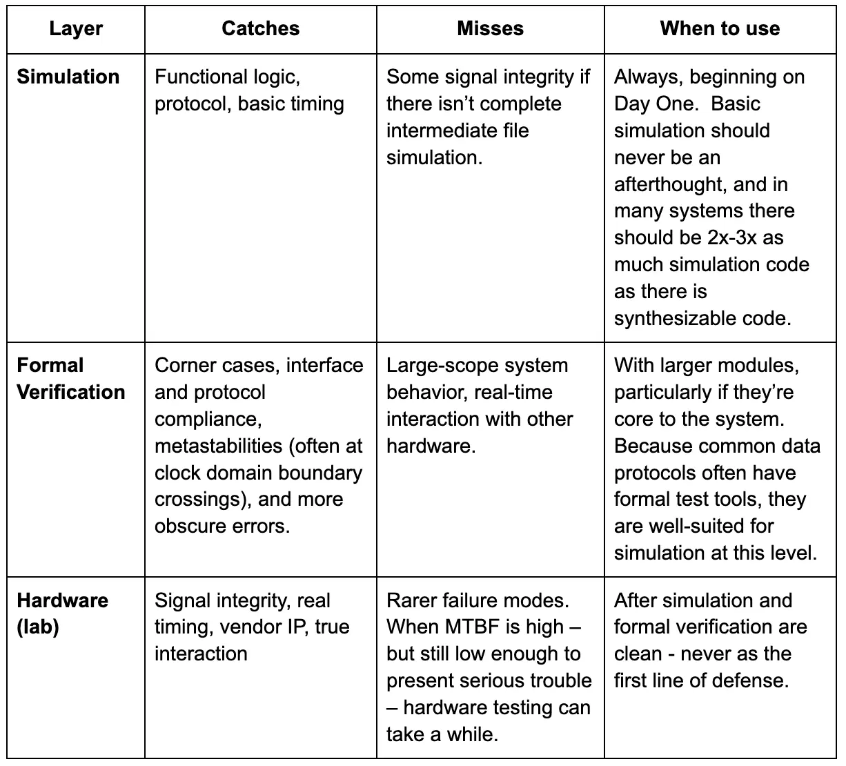
Leaning entirely on one layer is the common failure mode: simulation-only projects ship products that misbehave around vendor IP; formal-only programs miss integration bugs; lab-first teams burn months reproducing what should have been a five-minute simulation finding.
Testbenches: Where Most Projects Quietly Lose
Many FPGA projects don't fail when a bad testbench runs and produces waveforms, and the engineer eyeballs the output and moves on. Six weeks later, a bug surfaces in hardware, and the testbench, which is woefully incomplete, can't tell whether the bug is new or has been there the whole time.
The minimum bar for a serious FPGA testbench:
- Self-checking. Expected outputs computed in the testbench (reference model, scoreboard, or assertions) and compared automatically to the design's actual outputs. No human eyeballing waveforms.
- Constrained random stimulus alongside directed cases. Random inputs find bugs your assumptions hide.
- Coverage-driven. Code coverage and functional coverage points instrumented in the design, with regression runs until targets are hit. Coverage is what converts "we tested it" into evidence.
- Reproducible. Seeds logged. A failure today must be reproducible six months from now, after the engineer who saw it has changed jobs.
The framework you choose matters less than picking one and using it well:
UVM (IEEE 1800.2-2020) - SystemVerilog
Best for: Large designs, mixed FPGA/ASIC teams, complex protocol verification
UVVM
Best for: VHDL shops wanting modern methodology without SystemVerilog migration
OSVVM
Best for: VHDL shops needing advanced randomization and coverage
cocotb (Python)
Best for: Software-heavy teams, integration with Python tooling and CI
UVM is making inroads in high-density FPGA work the same way it did in ASIC design: it scales. cocotb is increasingly common in startup environments where the verification engineer is also writing the embedded firmware and prefers one language across the stack. The wrong choice is "no methodology" - bespoke testbenches that work for one person and nobody else.
Timing Closure Without Heroics
FPGA timing closure is the process of proving that your synthesized design meets its timing constraints - every flip-flop's input is stable before its clock edge, every signal arrives within its required window. And there’s nothing asynchronous that is going to produce a different outcome for a race condition when the silicon vendor moves from 28nm to 7nm technology to reduce manufacturing cost.
Static Timing Analysis (STA) - built into Vivado, Quartus, and every serious FPGA toolchain - checks setup time, hold time, and clock-to-Q across every path. The tool reports Worst Negative Slack (WNS) and Total Negative Slack (TNS). Negative slack means the design doesn't meet timing. Negative slack discovered the week before tape-out means somebody is redesigning some state machine or bit of combinatorial logic on a deadline.
The discipline that prevents it:
- Constrain early. Your SDC or XDC file is part of the design, not an afterthought. Define clocks, generated clocks, false paths, and multicycle paths as you write RTL - not when STA fails.
- Verify clock domain crossings. Most metastability bugs aren't synthesis errors. They're CDC bugs synthesis happily ignored. Aldec ALINT-PRO, Synopsys SpyGlass CDC, and Siemens Questa CDC find these - if you run them.
- Budget metastability. Mean Time Between Failures (MTBF) for a properly synchronized CDC is measurable and acceptable. For an unsynchronized one, it's roughly "when the customer demos it."
- Don't trust the warning list. "0 errors, 247 warnings" is not clean synthesis. Half those warnings are inferred latches, multi-driven nets, or clock-infrastructure mistakes that will surface in hardware.
The Right-First-Time FPGA Verification Plan
Right-first-time is a discipline, not a slogan. The discipline lives in a document: the FPGA verification plan, written before RTL synthesis begins.
A serious plan contains:
- Test plan. Every feature, interface, and operating mode mapped to the simulation, formal, or hardware test that exercises it. Untested features don't exist.
- Coverage targets. Code coverage (typically 95%+ for safety-critical work), functional coverage (100% of defined points), assertion coverage.
- Sign-off criteria. Specific, measurable conditions per layer: regression passes with N random seeds, assertions firing as expected, STA clean with a defined slack margin, CDC clean, lint clean.
- Traceability matrix. For DO-254 (aerospace), IEC 61508 (industrial functional safety), ISO 26262 (automotive) - every requirement traced to the artifact that demonstrates compliance.
- Tool flow and configuration management. Locked tool versions, locked IP versions, scripted regressions. A result that depends on which engineer's machine ran it is not a verification result.
The plan also defines what triggers re-verification. RTL change? Full regression. Timing constraint change? Full STA plus any test that interacts with that clock domain. Vendor IP version bump? Treat as a new design until proven otherwise.
<button onclick="window.location.href='/contact/'" style="display:block;margin:24px auto;padding:14px 28px;font-size:16px;font-weight:600;border:none;border-radius:6px;background:#e30613;color:#fff;cursor:pointer;">Talk to an FPGA Engineer</button>
The plan looks bureaucratic until the alternative shows up - usually at integration, usually late afternoon on a Friday. Improvisation in FPGA verification is how schedule slips happen.
When You Need More Than Simulation
Simulation has limits. Five situations where you need hardware in the loop:
Signal integrity. Your DDR or PCIe interface might pass STA and still fail in hardware because of crosstalk, reflection, or supply noise that simulation models can't capture. Same root cause as most high-speed PCB layout failures.
Vendor IP black boxes. Encrypted IP for MIPI, DDR PHYs, transceivers, and similar blocks doesn't simulate the same way it behaves in silicon. The vendor's Bus Functional Model (BFM) is an approximation. The real block is the spec.
Real-time interaction. Closed-loop systems - motor control, radio MAC layers, control-system feedback - depend on timing relationships with external hardware no simulator can model accurately. HIL rigs that emulate the external world in real time become the verification environment.
Long-duration behavior. Some bugs only surface after hours - soft-core firmware memory leaks, slow-burn metastability, accumulator drift. Simulation can't run that long; hardware can. Same applies to thermal and voltage corners: an FPGA at 85 °C on a noisy supply behaves differently than the same FPGA on the bench, and corner verification isn't optional for industrial, aerospace, and medical work.
Lab bring-up is the final verification gate. Treat it that way - not as the first place you discover what your design does.
What Verification Discipline Looks Like at Focus Embedded
We've shipped designs into environments where "respin" isn't a word anybody uses.
The cruise-stage electronics on the NASA Mars Rover didn't allow much room for a firmware update, and there was certainly no hardware update for a poorly routed PCB millions of miles away. The design had to be right before the launch vehicle was on the pad.
The 3M Picoprojector had a different problem: a consumer product with tight memory timing budgets and high component cost sensitivity, where a marginal design would have meant warranty returns at scale. Verification meant signal integrity simulation alongside RTL simulation, vendor IP integration testing, and bring-up against real display hardware.
Both shipped. Neither needed a respin.
That's what right-first-time looks like in practice: a verification plan written before the RTL, sign-off criteria you actually enforce, and engineers who treat lab bring-up as confirmation - not discovery. It's the posture we bring to FPGA / CPLD design engagements generally.
The Short Version
FPGA verification isn't glamorous. It doesn't ship features. It doesn't show up in demos. What it does is prevent the call from the customer site, the slipped quarter, and the engineering meeting where somebody asks how this got past testing.
If you'd rather not figure that out the hard way - we've done this before.
